
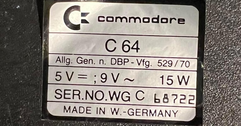
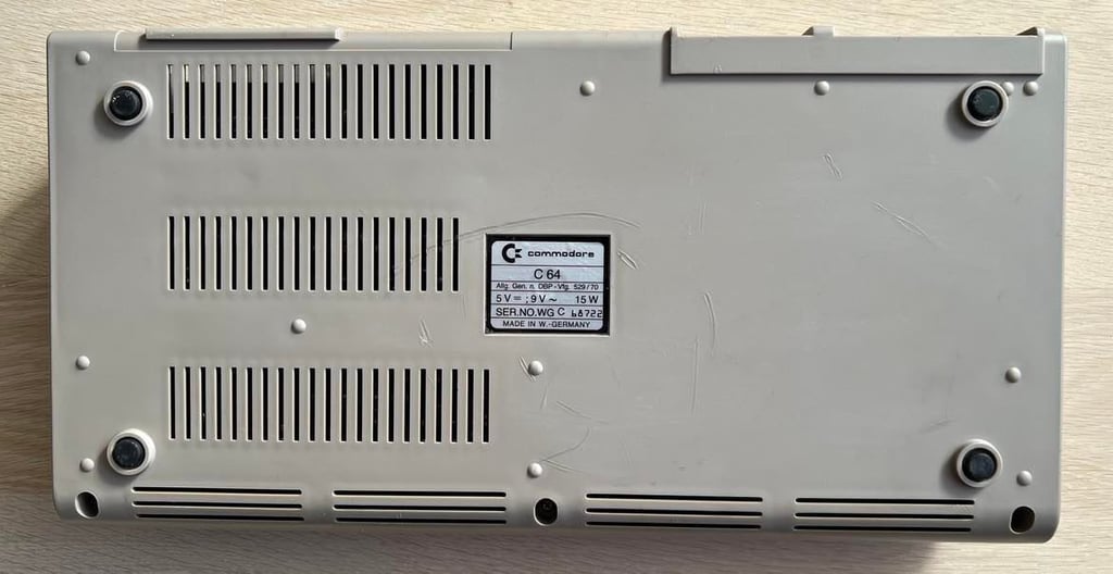
C64 Breadbin
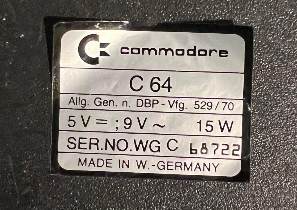
Ser. No. 68722
Assy 250407
Artwork 251137 (REV B)
Starting point
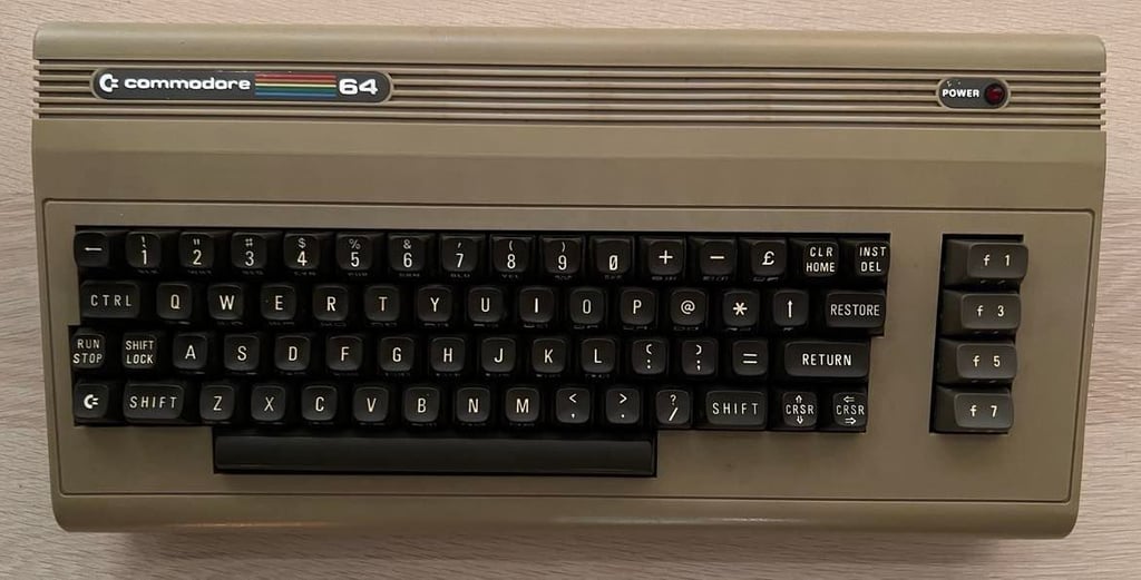
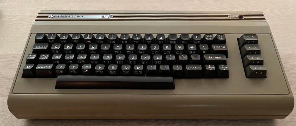
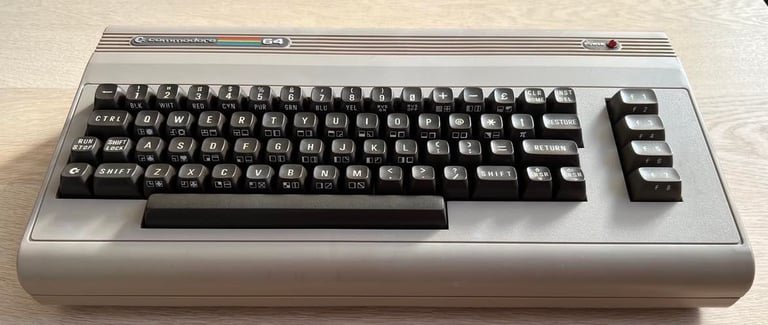
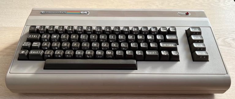
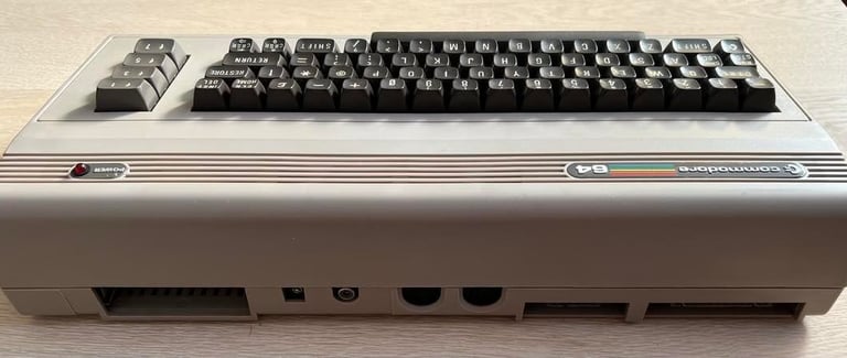
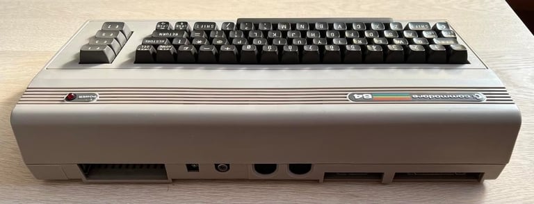
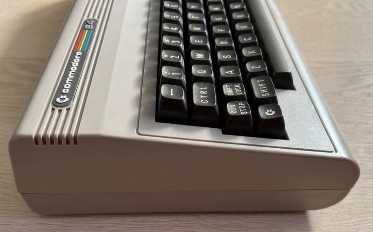
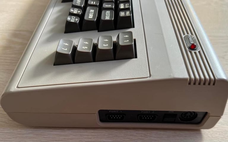
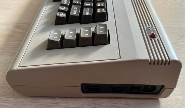
This C64C came to me as a request for refurbishment. From the exterior this Commodore 64 looks to be undamaged, but I already know that it is not working (black screen). It is a bit yellowed and there are some marks at the bottom. These marks occur when a cable (e.g. from a datasette) has been close to the plastic for several years. Nevertheless, with some cleaning and repair this could be a nice one!
Below are some pictures of the machine before refurbishment.


Refurbishment plan
To refurbish this C64 breadbin the plan is to do this trough the following steps (some of them in parallell):
- Clean and remove stains from the casing
- Clean and restore the keyboard
- Retrobright casing (and possibly the keys)
- Repair mainboard
- Replace electrolytic capacitors and voltage regulators. Add heatsinks and remove VIC-II RF-shield.
- Replace electrolytic capacitors in RF-modulator
- Verify operation by testing
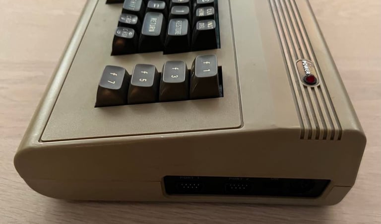
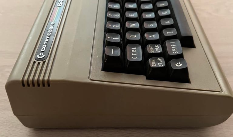
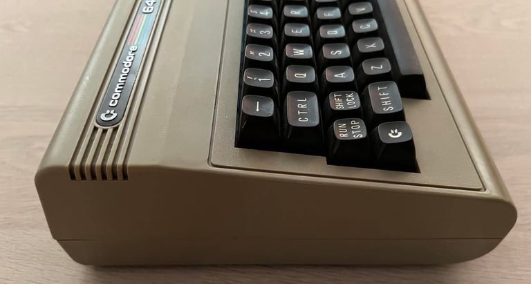
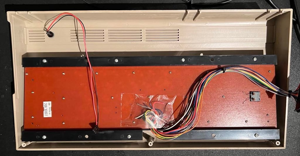
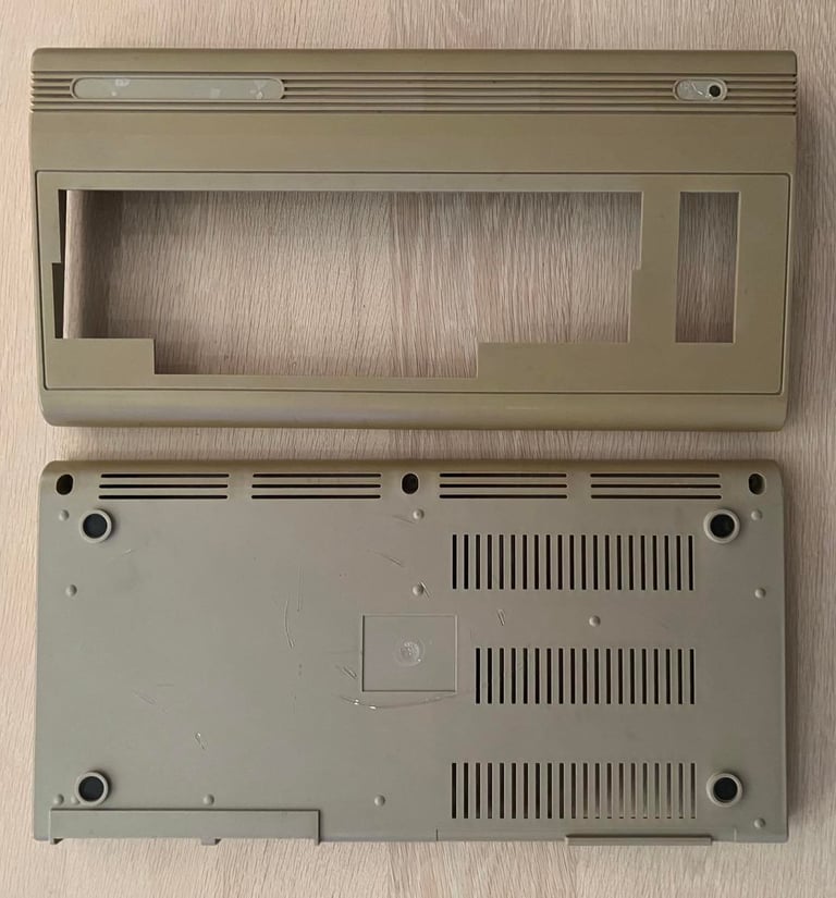
Exterior casing
The exterior casing consists of two parts; a top- and bottom cover. These are hold together by three screws at the bottom (just below the spacebar) and three plastic brackets on the back (inside the plastic casing). By removing these screws the inside is revealed. See picture below. The keyboard- and LED connector is removed to finally separate the top- and bottom cover.

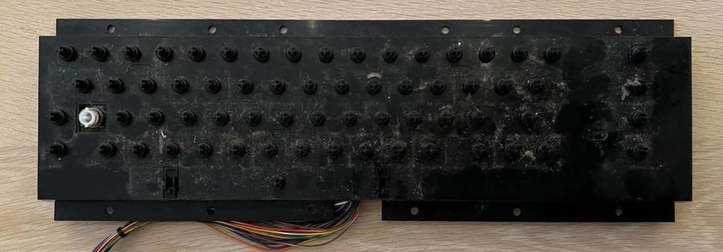
Next step is to remove the keyboard from the top cover. This is done by removing the eight screws around the backside of the keyboard. See picture below.

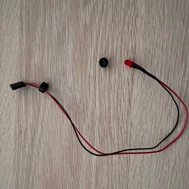
Then the plastic clip holding the LED is removed. This is done by first pulling away the first plastic ring surrounding the LED cable. With this out of the way the LED is pushed from the from the front toward the back - the LED will pop out. Then the last plastic clip is pushed from the back towards the front. These plastic parts are old and brittle so its wise to be very careful not to brake them.
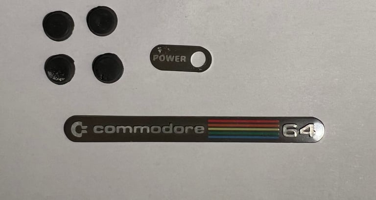
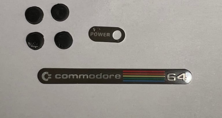
The "Commodore 64" and "Power" badge is removed from the top cover, and the serial number sticker is removed from the bottom. This is done by using some hot air from a hair dryer, and carefully removing them with a small sharp knife. The reason for removing the badges and sticker is to make sure they are not damaged during cleaning and retrobrighting.
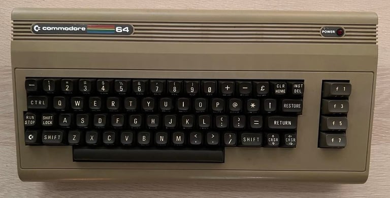
Top- and bottom cover are now ready for cleaning and retrobrighting. Picture below shows the plastic covers before refurbishment.

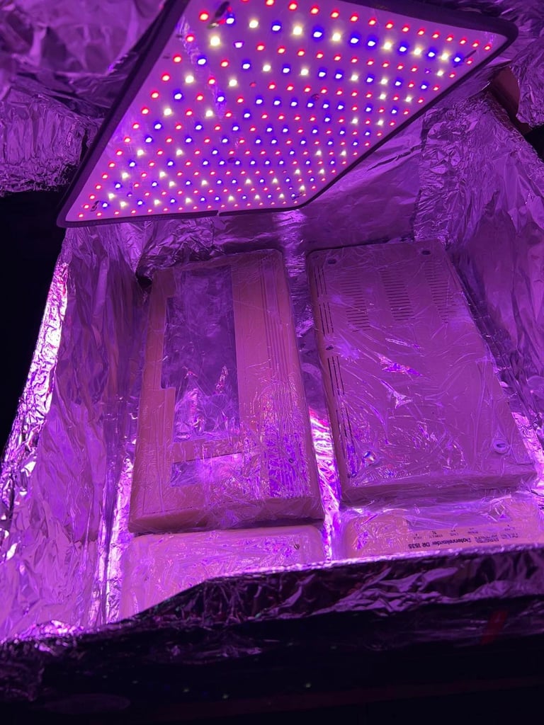
Retrobrighting is done by applying 12 % hydroperoxide cream for about eight hours. The plastic parts are wrapped in cling film, and the hydroperoxide cream is re-applied about each hour - and the parts are exposed in UV-light.
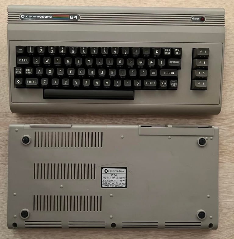
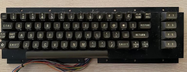
Below is the result from retrobrighting and with all stickers/badges put back. Also the cleaned and retrobrighted keyboard is in place. I think the result was very good!

Keyboard
The keyboard looks to be undamaged and in general good condition. It is a bit dirty, and with a normal amount of dust and grease - but otherwise the keyboard looks fine.
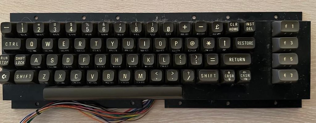
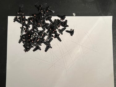
All keys are removed with the keycap puller and placed in a bowl of mild soap water for a few hours. Note that beneath each key is a little spring, but that the spring beneath the spacebar is different from the rest. So it´s a good idea to keep this spring separate from the rest. The plastic casing for the keys also looks undamaged and in good condition. Some dust and dirt, but no visual damage.

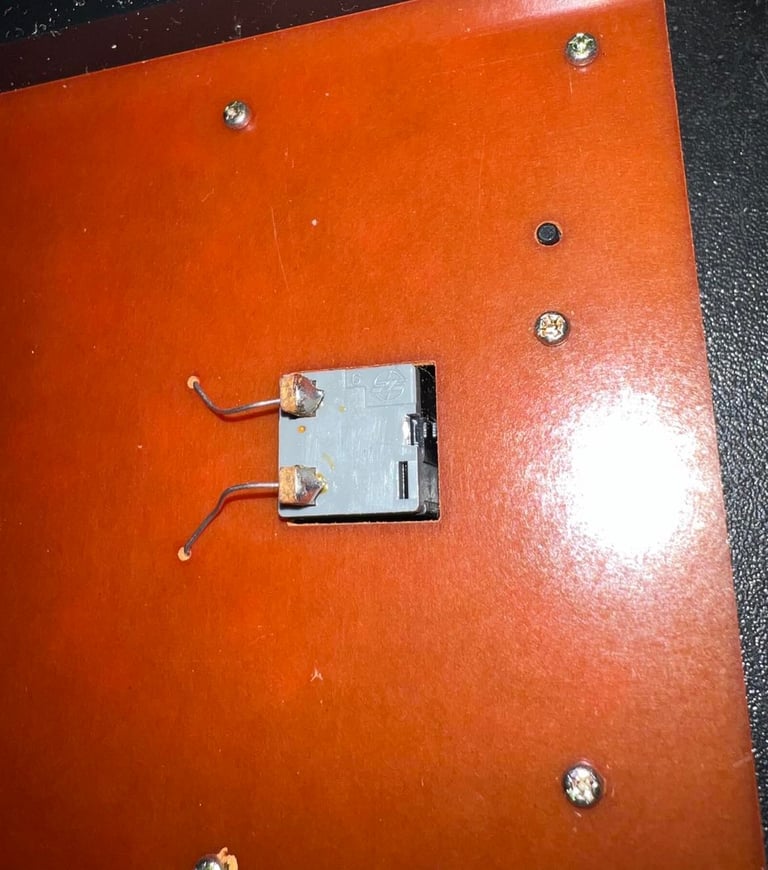
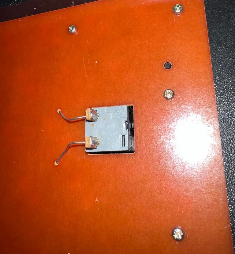
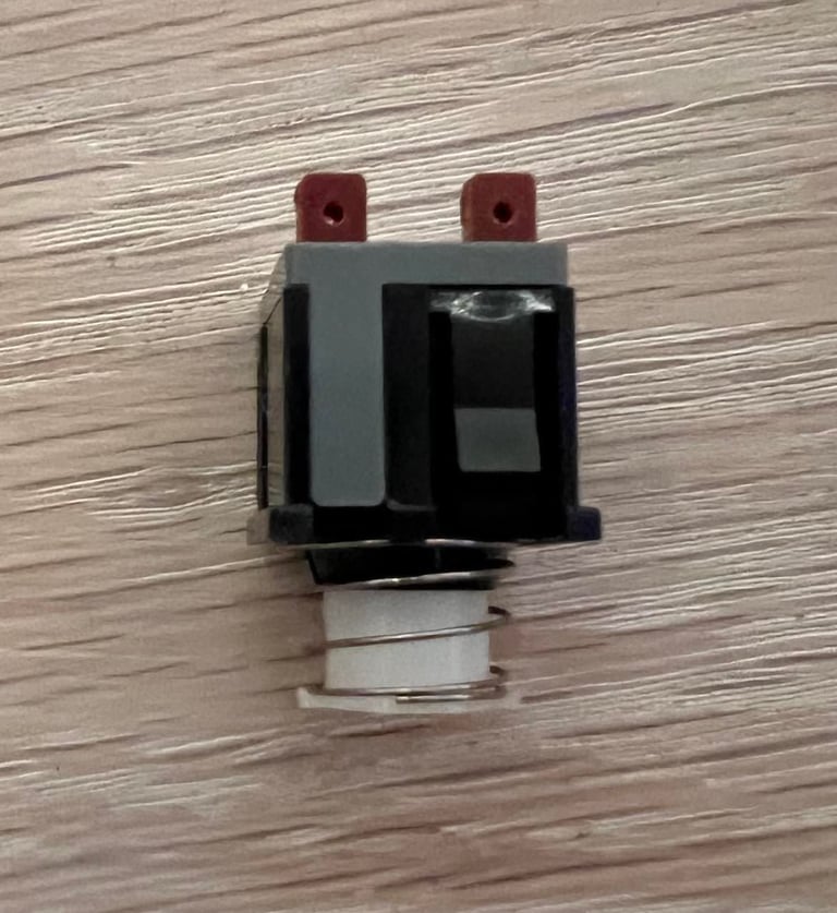
Before the keyboard PCB is unscrewed the SHIFT-LOCK key is removed. Two wires are soldered to the SHIFT-LOCK on the backside of the keyboard. These are desoldered and the SHIFT-LOCK is removed by pushing it firmly forward (from the backside of to the front of the keyboard).

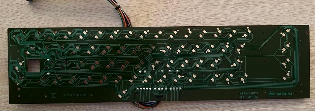
The >20 machine screws holding the PCB are removed from the backside of the keyboard chassis. The PCB show that this is a MITSUMI keyboard (version KSR-A66Y). There are no signs of corrosion, or broken traces, on the board. After cleaning the PCB with isopropanol it looks very good.

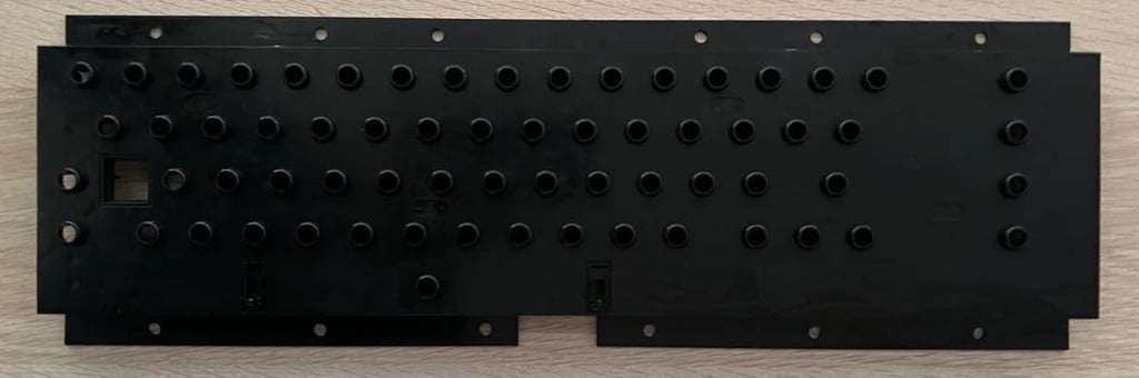
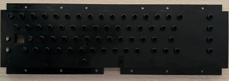
All plungers are removed from the keyboard plastic chassis, and this chassis is cleaned with mild soap water. There are no visual damage / cracks on the chassis so it appears to be in perfect order.
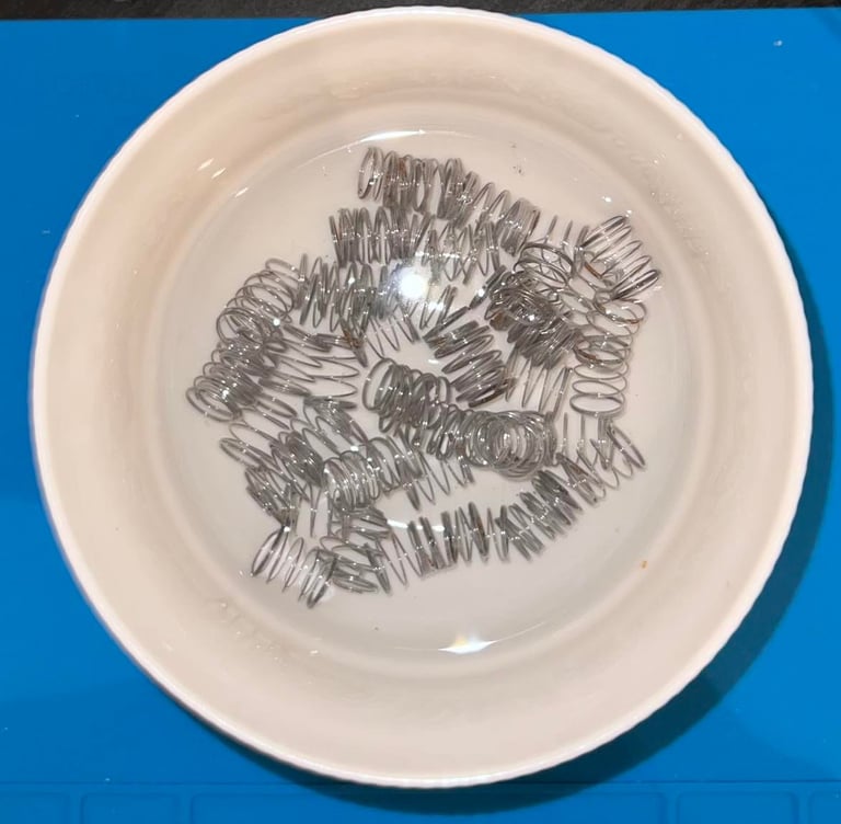
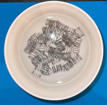
The springs looks good, but as good practice all are placed in a bowl of vinegar for an hour to remove any corrosion.
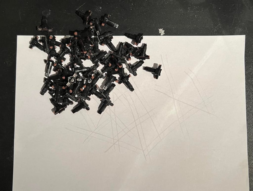
To revive the key plungers I use a little trick: the plungers are carefully dragged on a clean paper. This will remove the old grease and debris on the plungers. I find this method more gentle than cleaning them with isopropanol. And the effect is usually very good - they will be good as new.
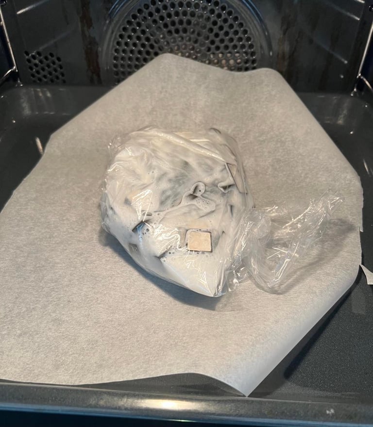
Keys are placed in a bag of 12 % hydroperoxide cream for two hours in 50 degrees Celcius to retrobright them slightly.

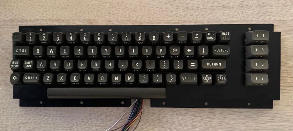
Finally the keyboard is re-assembled. See result below.
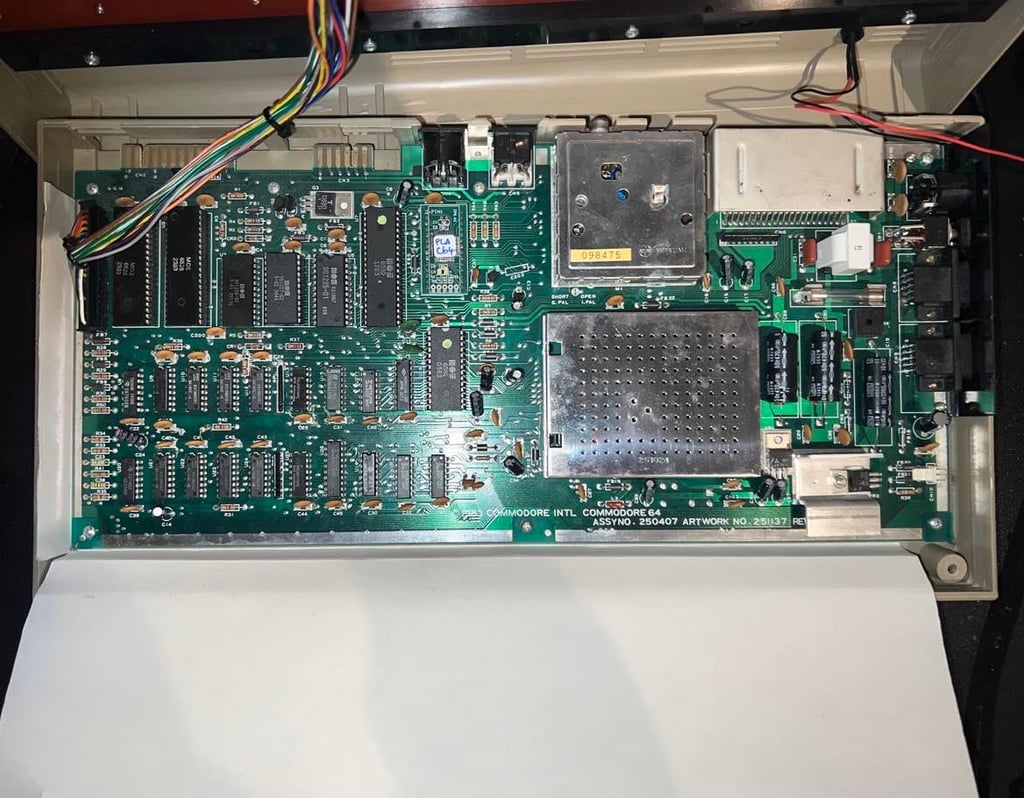
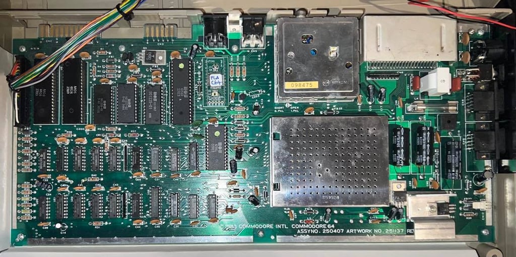
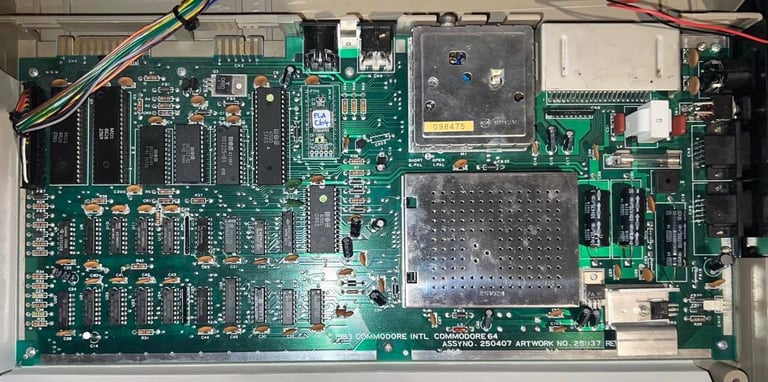
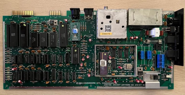
Mainboard - REPAIR
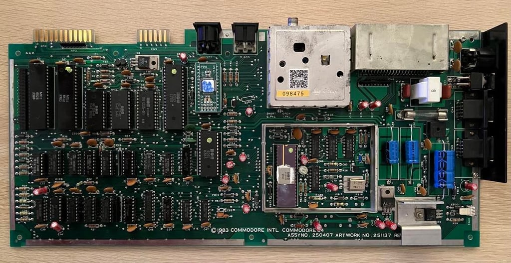
This is an assy 250407 artwork 251137 REV B mainboard. As previously mentioned this mainboard is reported to not work - only displaying a a black screen. So the plan is to repair the mainboard before continuing with other refurbishments such as replacing capacitors and voltage regulators.
Below is a picture of the PCB before the repair.
Intial troubleshooting
First step in the fault finding process is to check for any short circuit and then check voltages. I can´t find any short circuits when measuring with a multimeter pin #1 and #2 (5 V DC from PSU) and pin#10 and #11 (9 V AC from the PSU) on the user port. Also, there are no short circuit on the 7805 and 7812 voltage regulators. This means that is should be OK to power the machine on. I use a modern PSU to power the Commodore 64. But before I power on I remove the SID chip. This is not required for the Commodore 64 to boot up. Also, these are very rare these days so I don´t want to break this SID by accident (I don´t know if it works yet, but anyway...).
Result is (as I already know) a black screen. But it does seem to produce a valid video signal (composite) - so there is good hope that the VIC-II is working.
Next step is to feel the temperature on all the chips to see if any of them are very hot (or hotter than normal). Result is that none of the chips are specially hot so I don´t get any clue on what is wrong here.
Voltages are measured on the mainboard (see table below). All of these are within acceptable range.
Visual inspection
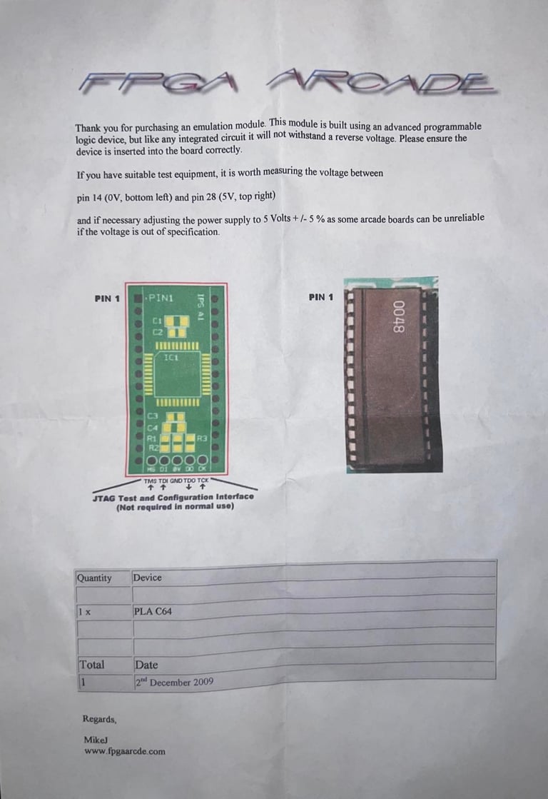
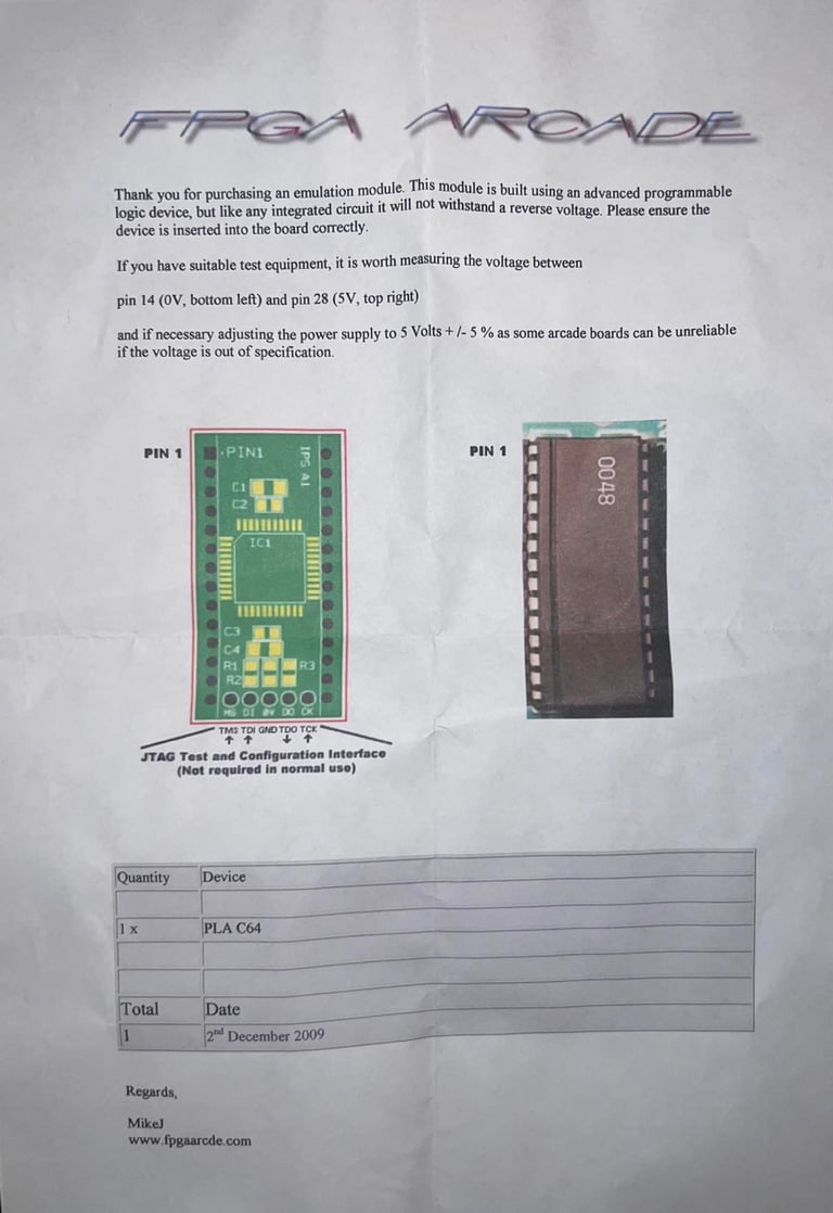
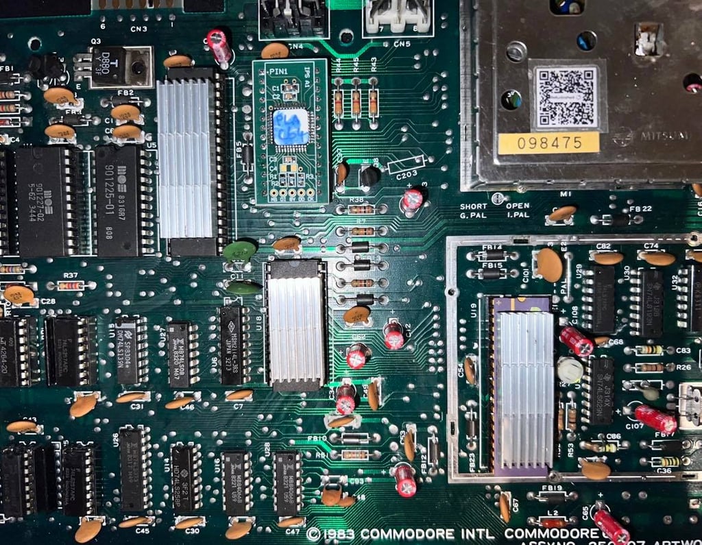
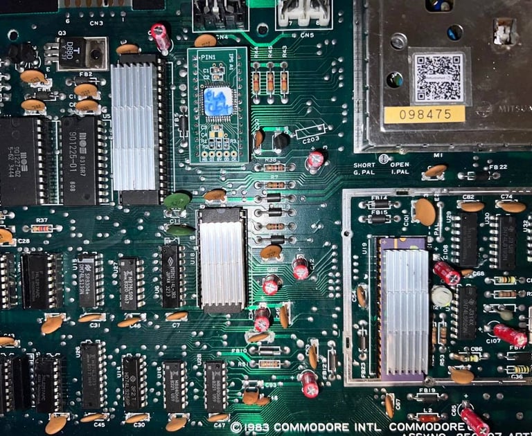
There are no visual damage on the board - no signs of corrosion, broken traces (on either back or front of the PCB), no leaking caps, no melted chips or voltage regulators. The original PLA is replaced with a modern PLA FPGA chip which is very welcome. Original PLA chips fail notoriously.
The following chips are installed on the mainboard before repair:
It is nice to see a new modern PLA replacement since the MOS PLA is well known for failing. The instructions for the replacement PLA is dated 2nd December 2009 - see picture below (click to enlarge). In the instructions it is stated that the voltage supplied to the PLA should be measured to be +5V (+/- 5%). Using a multimeter I measure this to be 5.06 V which is fine so problem there.
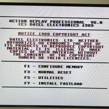
Introducing the dead test cartridge
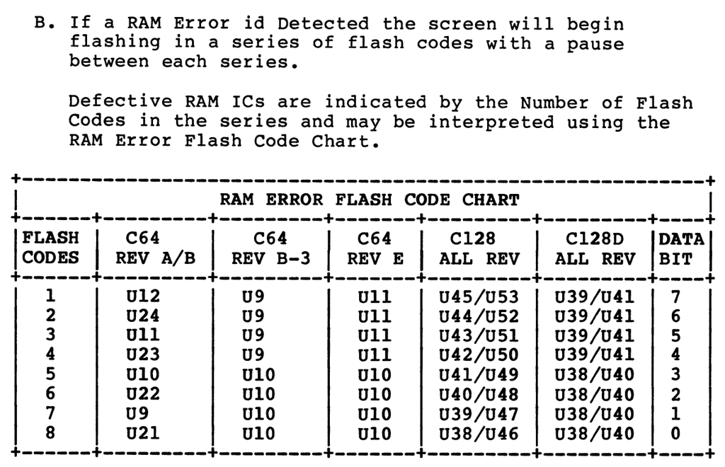
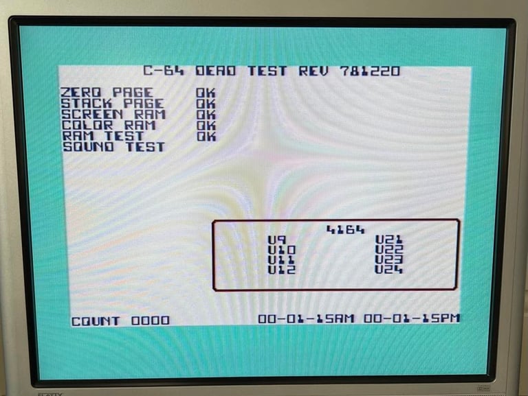
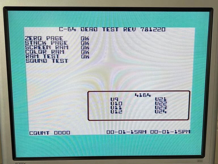
The dead test cartridge can give hints about what is wrong with the machine. As long as the CPU, PLA and VIC-II is working (or partially working) the cartridge will try to run its test software. Chips such as Kernal, BASIC, CharacterROM, CIA #1 and #2 does not need to work for the cartridge to operate. The Kernal, CIA #1 and CIA #2 are socketed so these are removed. With the dead test cartridge in place I get the first hint on what is wrong with the machine: I get a flashing screen. At it flashes only once each interval - see video below.

In the dead test cartridge manual there is a list explaining what the flashes represent. As seen in the table below the single flash represent a potential fault in RAM chip U12.
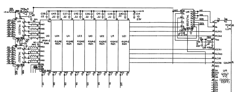
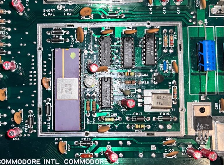
If the RAM at U12 was a "MT" branded chip, or was very hot, I would replace this immediately as the dead test manual suggest. But these are NEC chips, and as far as I know they are not prone to fail. So I choose to first investigate if there could be a conflict on the address- or data bus using the oscilloscope. Also, I use the oscilloscope to check for any irregularities around the glue logic used for the RAM memory handling 74LS258, 74LS257 and 7406. In the schematics below you can see how these chips are connected to the RAM chips.

Next test is the "Piggyback" method. I use a known good RAM chip and place this directly on top of the PCB mounted RAM chip. It is important that the legs are aligned with the top- and bottom RAM chip, and also applying enough pressure by pushing with my finger to make sufficient contact. I try this method on all the eight RAM chips, but I get no difference. Always just one flash.
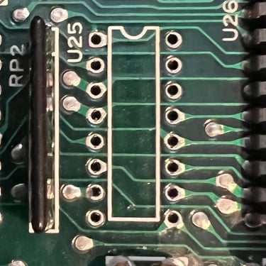
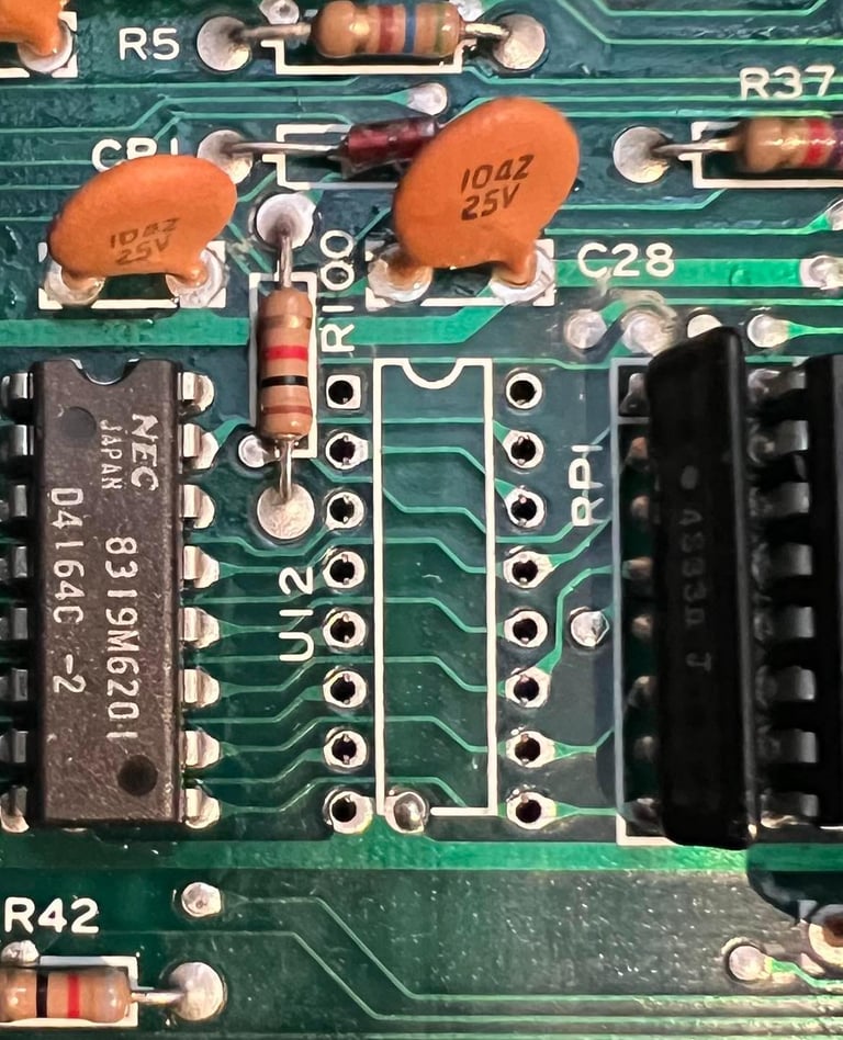
Before starting to replace potentially broken RAM chips I choose to desolder U13, U25 and U8 (glue logic). Even if I can´t see anything wrong here with the oscilloscope, I have seen several times before that these can fail. So it is good to have them checked and socketed anyway. No traces or pads are damaged during this operation. Note that when I test these I replace these chips temporarily with known good chips. If I detect no change with the replaced chips I put the old ones back. The result is (no surprise): still the same "one flash". Below is a picture from the desoldering of these chips (click to enlarge).
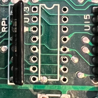
Next step is to desolder U12 (RAM). This is the chip indicated to be bad by the dead test cartridge. The chip is desoldered, a socket is soldered in and a known working RAM chip is installed. Below is a picture from the desoldered U12. No pads or traces damaged during the operation.

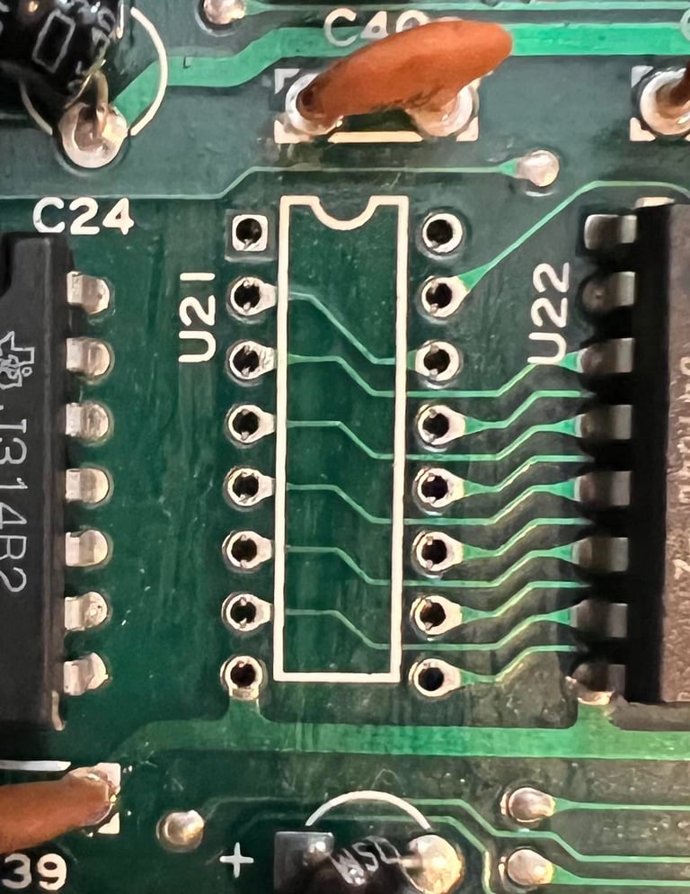
And the result is: progress! It is no flashing eight times - which points to U21. So I desolder this chip, install a socket and test with at known working RAM chip. Below is a picture of the desoldered U21. No pad or trace lifted.
Still making progress now. The flashing now stops and something that looks like the dead test user interface appear. But the font is missing and it crashes after the 2nd test. How come? Two RAM chips gone? Are even more RAM chips gone?
In the video below the result is shown.
It seems like the dead test cartridge starts to work, but there are two clues:
The font is corrupted. The dead test ROM cartridge contains its own font - which is probably copied to C64 RAM during boot-up.
The 1st looks to be completed. The 2nd seems to crash before the picture is completely changed.
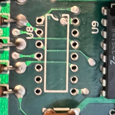
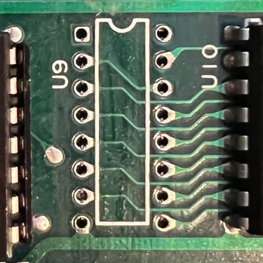
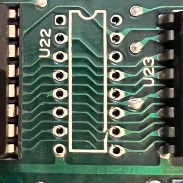
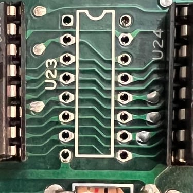
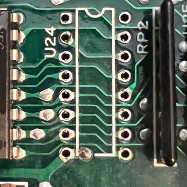
To me this points in the direction of a marginal RAM chip. A RAM chip which is not totally dead, but have some memory areas which are corrupt. I know the two previously installed are working (also doble checked in a working C64), so I will start the hunt looking for the culprit. I start with the "piggyback" method: placing a working RAM directly on top of the RAM on the PCB. This sometimes work, but I get no result with this method. So I need to start desolder, socket and test one RAM chip at the time: U9, U24, U22, U23 and U11. Below are pictures from the desoldering of these (note: I forgot to take a picture of U11) - but no pads or traces were lifted on any of these.

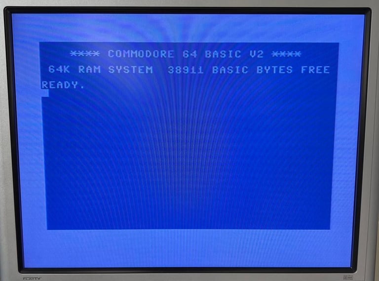
After replacing U11 with a working RAM - success! The dead test cartridge then runs all the tests with visible fonts! The SID and CIA tests doesn´t pass of course since these are not installed (yet). All chips are then put back in (including the SID) - and the Commodore 64 is turned on. Result is shown below!
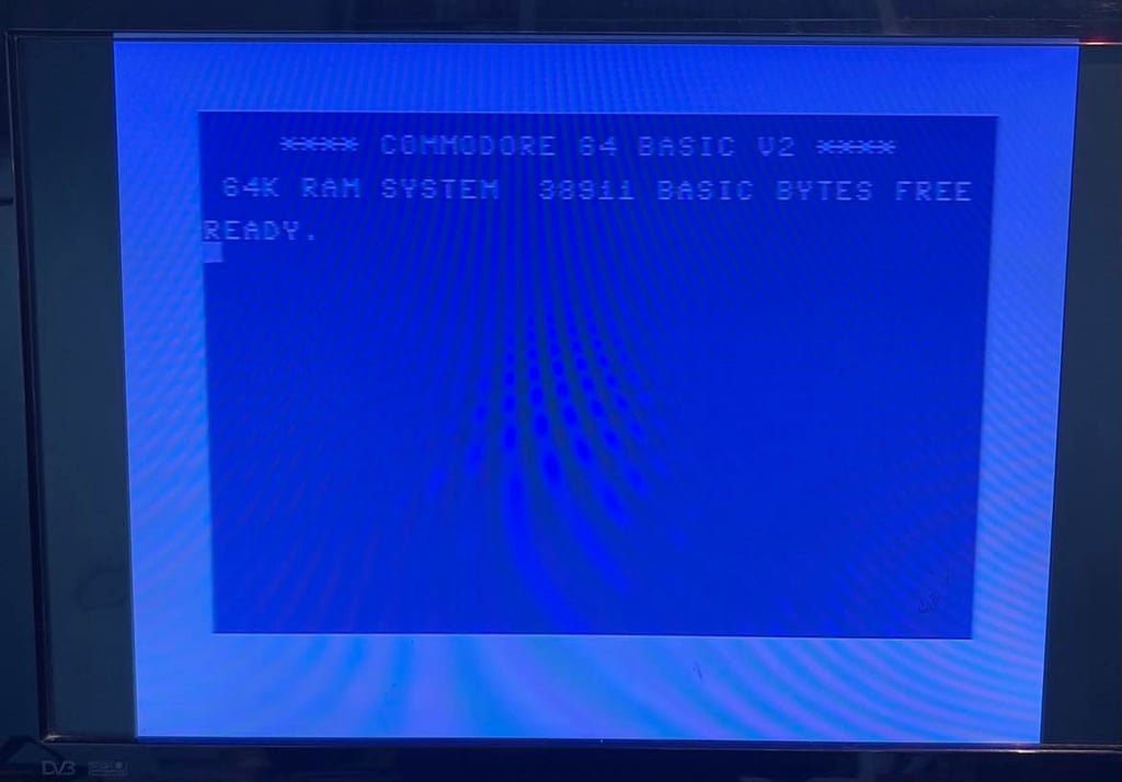
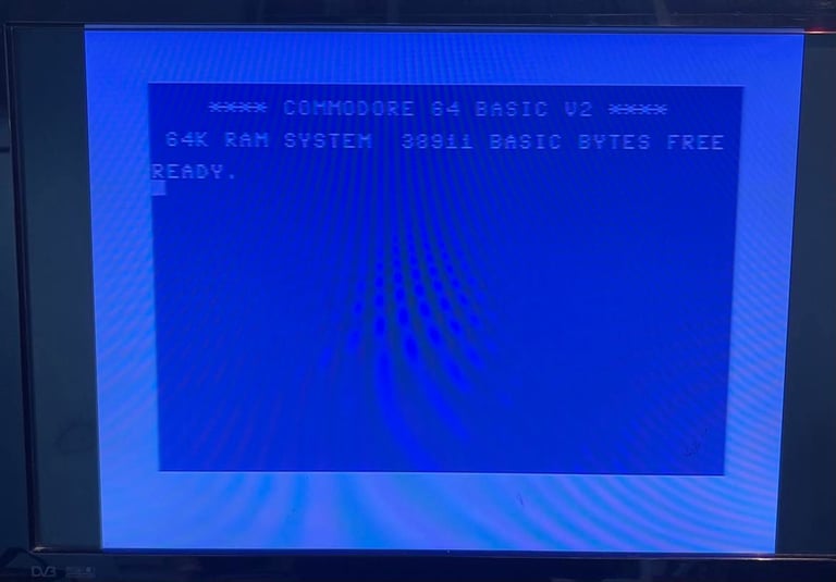
38911 BASIC BYTES FREE! This looks very good! It doesn´t mean that the Commodore 64 works 100 % yet, but it concludes the repair section. RAM chips are ordered from retroleum.co.uk to replace the broken ones.
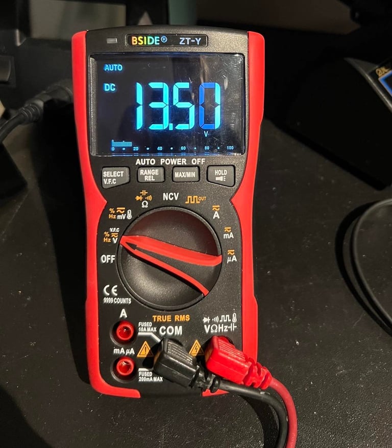
It is a but of a mystery who three RAM chips were broken at the same time. Something seems to have created havoc in these chip. I check the voltages produced by the original PSU which followed the Commodore 64. The 9 V AC is fine (about 11 V AC), but the 5 V DC is ... 13.5 V (!). This is obviously very high, but I guess this high voltage has occured very late. If the machine had been powered with + 13 V DC I believe that most of the MOS chips would be gone. Anyway, the machine looks to be repaired so I will continue with rest of refurbishment.
NOTE: For some reason I see that I forgot to mention that I also socketed the BASIC ROM chip during the faul finding. I did this to make sure that this ROM chip did not pull down the address- or databus in any way.
Mainboard - REFURBISH
Replacing the electrolytic capacitors
It is good practice to replace the electrolytic capacitors on the mainboard. These capacitors are used for smoothing voltages/ripples and filtering purposes. It is not strictly required to do this (unless the capacitors are leaking), but the capacitors are almost 40 years old. And due to age they tend to alter their capacitance (and resistance) which could cause the Commodore 64 to behave odd. A bad capacitor is not harmful in any way, but it could cause instabilty.
All the electrolytic capacitors on the mainboard is replaced with quality capacitors. An overview of required capacitors are found in the reference bank for capacitors.
NOTE: The 2 x 470 uF capacitors are replaced with 25 V voltage ratings. On the original board these were rated to 50 V, but the communities guess is that this was done by Commodore due to supply. It is perfectly fine to use 25 V rating. Read more here.
Below is a picture of the mainboard with the new electrolytic capacitors on the mainboard.
Before replacing the voltage regulators I remove the RF-shield casing for the VIC-II area. The RF-shield is no longer required in modern times, and the only "function" it does now is to encapsulate heat. And this is something which is not fortunate for old MOS chips... so therefore the RF-shield is desoldered. Note that in the picture below there are some wet marks which is only some isopropanol residue from the cleaning.
Replacing the voltage regulators
There are two voltage regulators on the C64 mainboard; one for 12 V DC and one for 5 V DC. These voltages are used for the SID- and VIC-II chip (read more about the different voltages on the mainboard). The reason for changing these are to reduce the risk for destroying the SID- and VIC-II chips. These are getting rarer each day and they are fragile to voltages which are higher than normal. And since the 7805 (+5V) and 7812 (+12) voltage regulators are almost 40 years old it is wise to change these.
Below is a picture of the new voltage regulators installed. Note that it is only the 7805 voltage regulator which is mounted on a heat sink. This is from factory. Also, between the 7805 and the heat sink there is a small drop of heat paste for better transferring the heat. The 7812 is not mounted with a screw on the mainboard (which is normal).
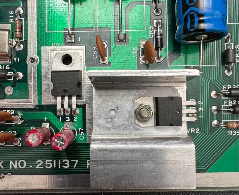

Adding heat sinks
Some important chips can run very hot; SID, VIC-II and CPU. And heat is one of the factors which can reduce the lifetime of these chips so adding heat sinks can reduce the probability of these chips failing. In the picture below the chips have the heat sinks installed (CPU to the left, SID in the middle and VIC-II to the right).
Before desoldering the RF-modulator the user- and datasette port is thoroughly cleaned. This is done by first rubbing the contacts with an rubber eraser and then cleaning the contacts with isopropanol and Q-tip.

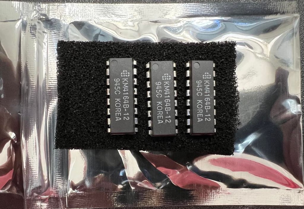
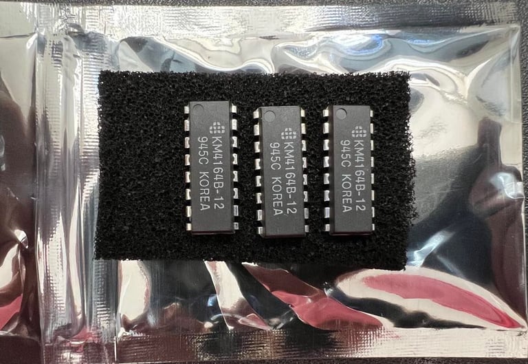
New RAM chips arrive from https://www.retroleum.co.uk/. These are installed and the table of measured voltages (in previous chapter) is updated.
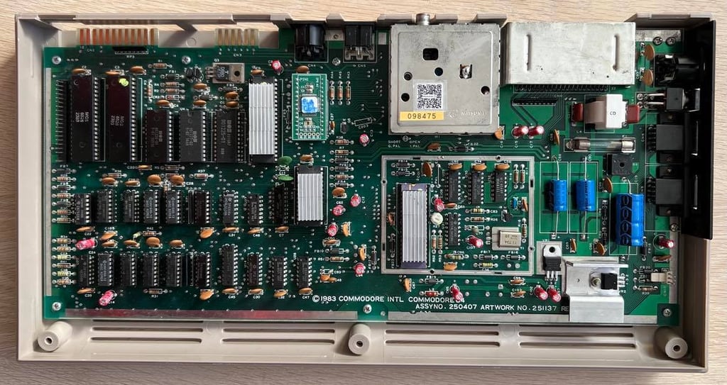
Below is a picture of the mainboard after the refurbishment - with new RAM chips, chips in sockets, new capacitors on both mainboard and RF-modulator and voltage regulators.

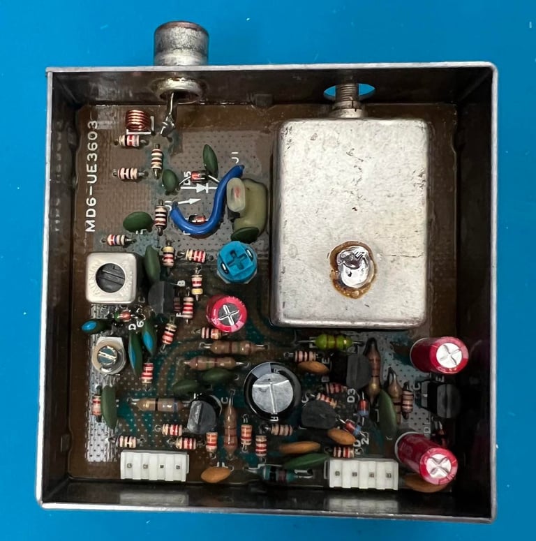
RF modulator
There are four electrolytic capacitors in the RF-modulator version MD6-UE3603.
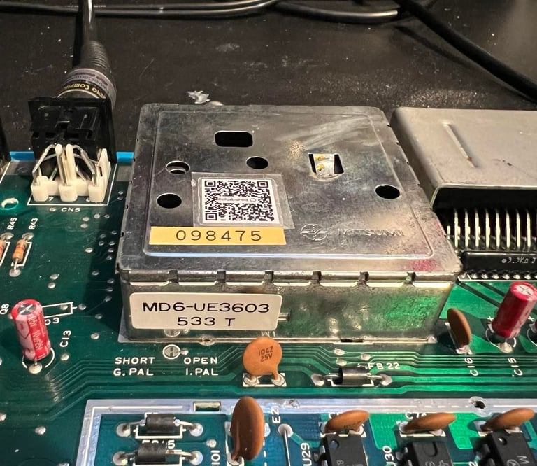
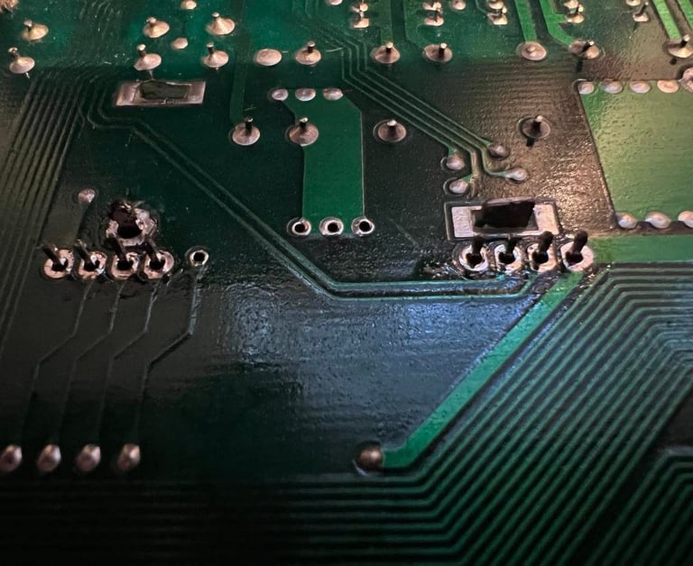
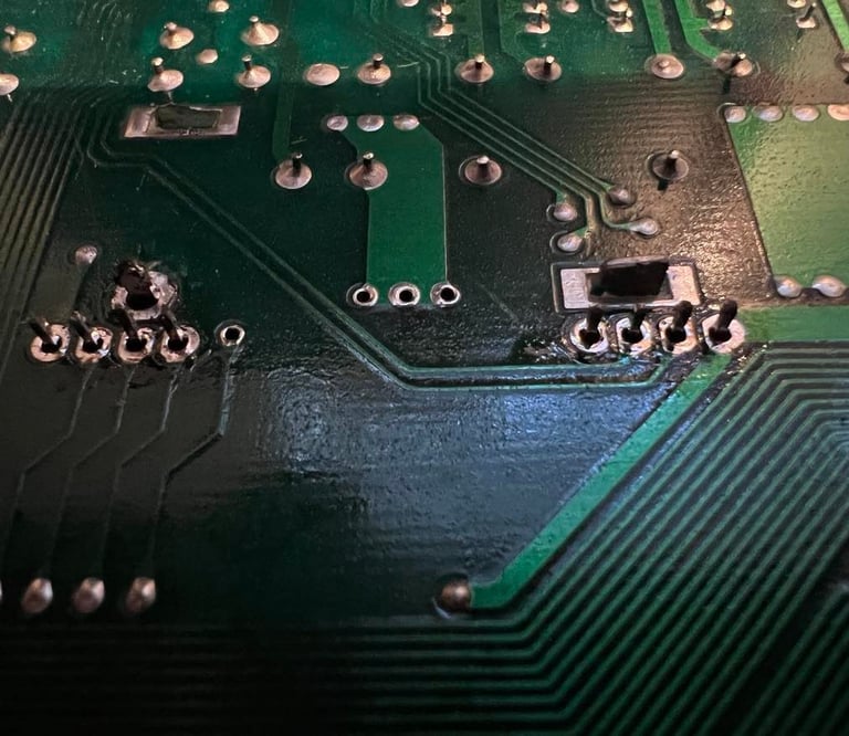
It is not trivial to desolder the RF-modulator. The PCB inside the RF-modulator is "floating" on eight pins which are soldered onto the mainboard. And in addition there are four thick pins which connects the RF-modulator container/can to the mainboard. So when desoldering the RF-modulator it is very important to be patient - if you rush this you will probably rip some traces or pads. I use both desoldering iron, soldering iron and hot air to remove the RF-modulator. Below are som pictures from the desoldering process.
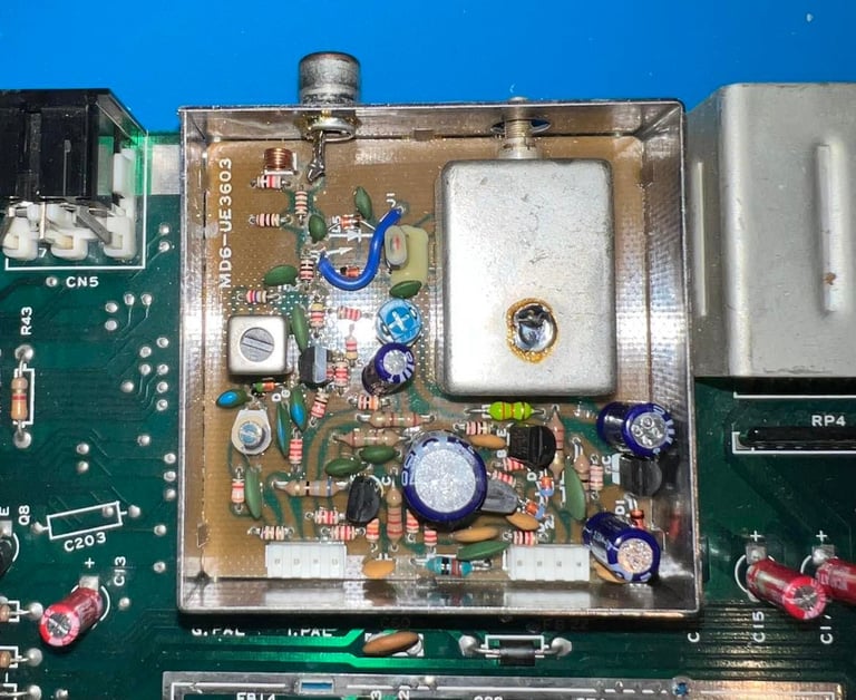
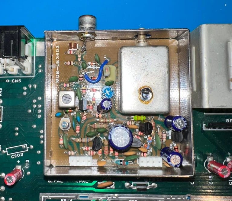
No pads or traces are lifted, and the four capacitors are replaced with quality brand caps; 1 x 10 uF [16V], 2 x 100 uF [10V] and 1 x 470 uF [10V].

Testing
Final stage - testing that the Commodore 64 works as it should. To test the machine I do this in two main stages:
Basic functionality testing of CPU-, SID-, PLA-, VIC-, RAM- and CIA chips. In addition keyboard is tested.
Extended functionality testing using all aspects of the machine
Basic functionality testing
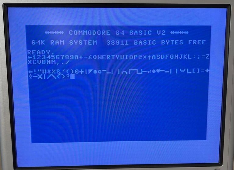
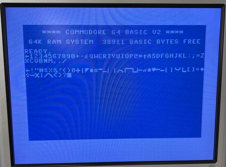
First test is to turn the machine on and make sure the classic blue screen is present with all 38911 BASIC BYTES FREE. Result: PASSED.

Next step is to check that the keyboard is working and that all keys register the input. Result: SUCCESS.
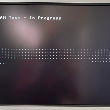
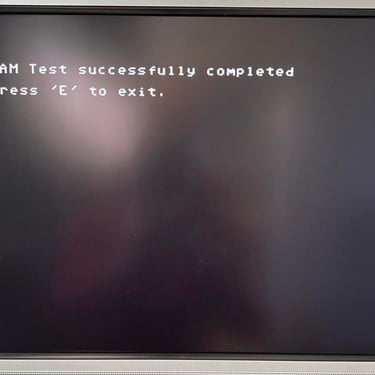
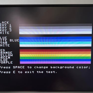
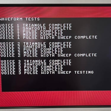
The dead test cartridge is used to check the basic functionality of the CPU-, VIC-, CIA-, PLA-, and RAM chips. Result: SUCCESS.
Last part of the basic functionality testing is to use the 64 Doctor software and the Commodore 64 SID tester software. This is to test the RAM-, SID- and VIC-II chip to some more extent. Result: SUCCESS.
Extended functionality test
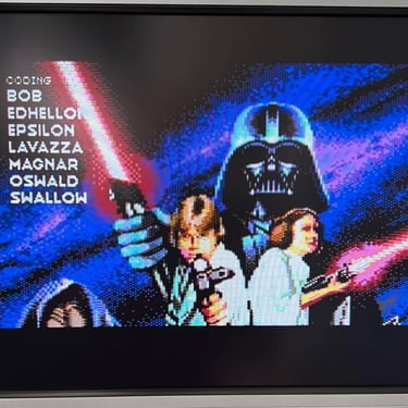
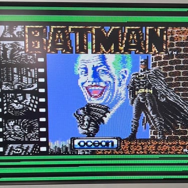
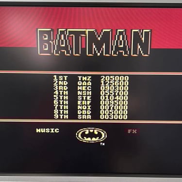
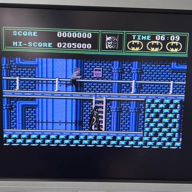
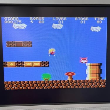
To test the Commodore 64 thoroughly I use the Ultimate II+ cartridge. This cartridge can emulate both cartridge, diskdrive (1541) and datasette. With this installed I test several games and demos - loaded from both disk and datasette. Below are some pictures from the testing. I can not find any issues / problems during testing. Result: SUCCESS.

Final result
"A picture worth a thousand words"
Below is a collection of the final result from the refurbishment of this C64. Hope you like it! Click to enlarge!


"Are you keeping up with the Commodore? 'Cause the Commodore is keepin up with you!"
Below is a video of the Commodore 64 back home at the customer together with the refurbished datasette and Wico Commander Control!

Banner picture credits: Evan-Amos