

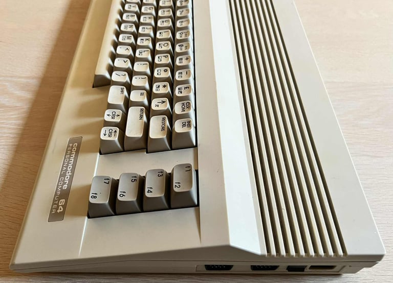
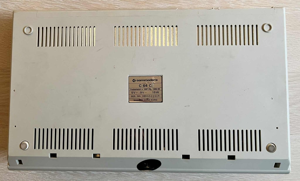
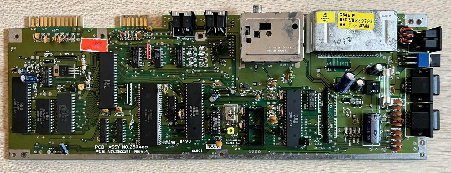
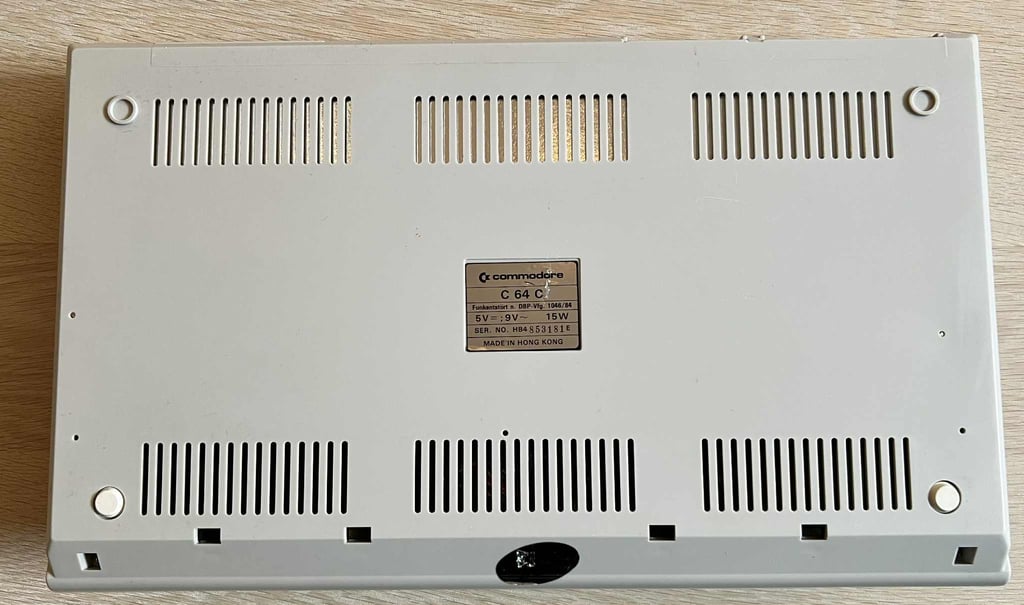
C64C [PAL]
Ser. No. 853181
Assy 250469
Artwork 252311 (REV 4)
Starting point
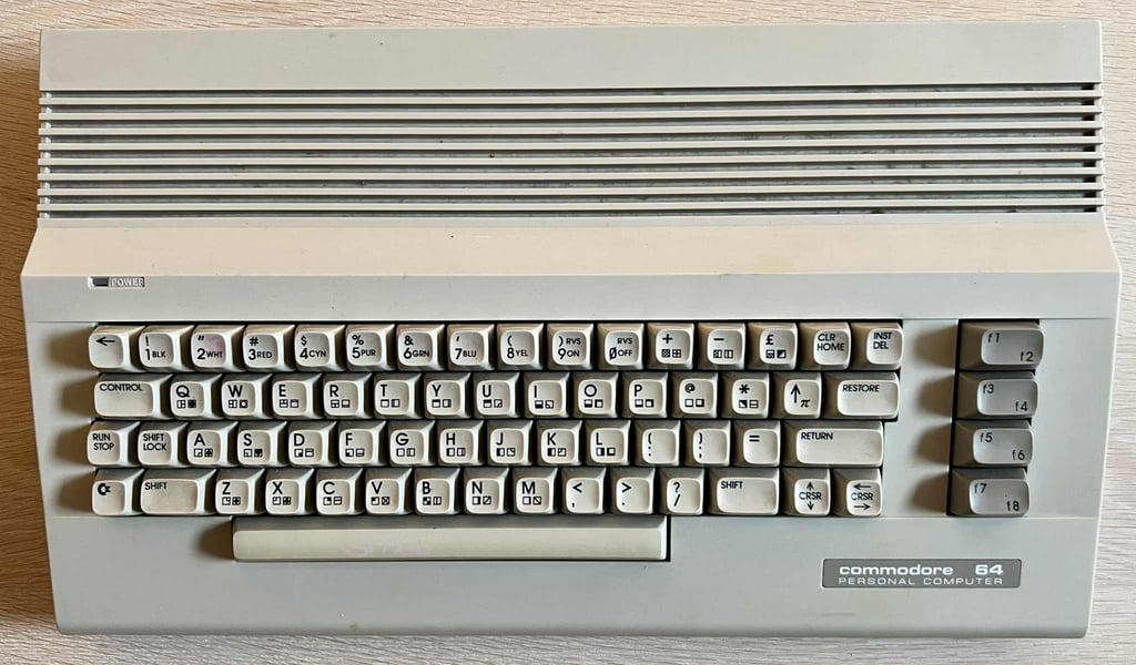
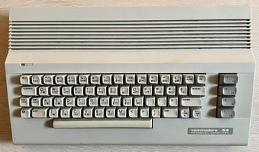
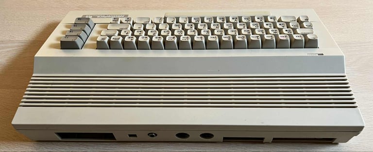
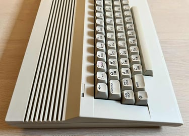
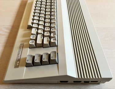
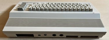
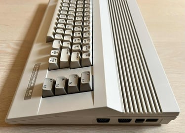
On the bright side this C64C appears to be only slightly yellowed and the warranty seal has not been broken! But, oh my, it is incredibly dirty. I do not think that the pictures below doesn´t do it justice - it is way more dirty than it looks. There is a lot of dust in the grooves on the top part of the machine, and I can see plenty of grime beneath the keycaps and there are quite a lot of marks on the covers.
The power switch is completely stuck in "ON" position, so that needs to be fixed. Also, it does seem like the protective film on the "Commodore 64 personal computer" badge is still on. Nice!
Does it work? At the moment I have no idea.
All in all, I think that this can turn out to be a very nice C64C. Below are some pictures of the machine before refurbish.


Refurbishment plan
The refurbishment plan for this C64C (order can vary and some of the tasks will be done in parallell):
- Refurbish the covers (clean, repair if required and retrobright)
- Refurbish the keyboard (clean, repair if required and retrobright)
- Refurbish main board (clean, check and repair if required)
- Verify operation by testing
The plan can be updated during the refurbishment process. Sometimes I discover areas that needs special attention.
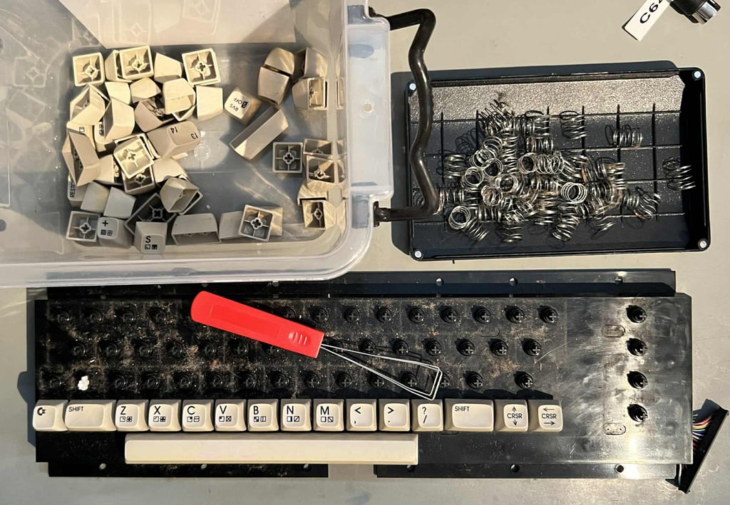
Disassembly
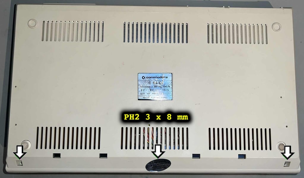
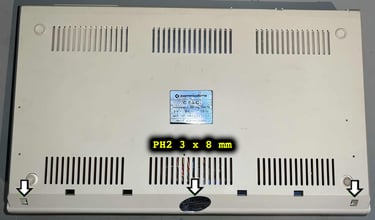
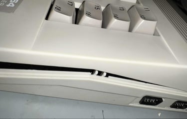
First step of the disassembly is to remove the three screws at the bottom of the C64C. These are PH2 3 x 8 mm screws. NOTE: when removing the screws make sure to not use a big screwdriver with high torque. The warranty seal is now broken... probably after 35+ years!
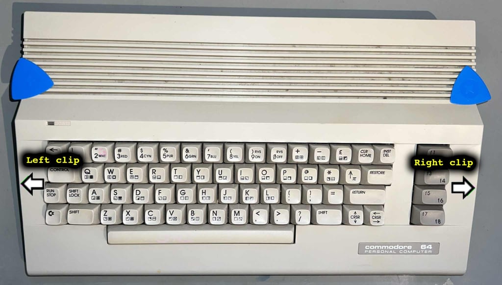
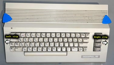
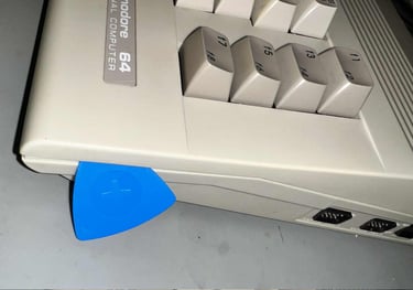
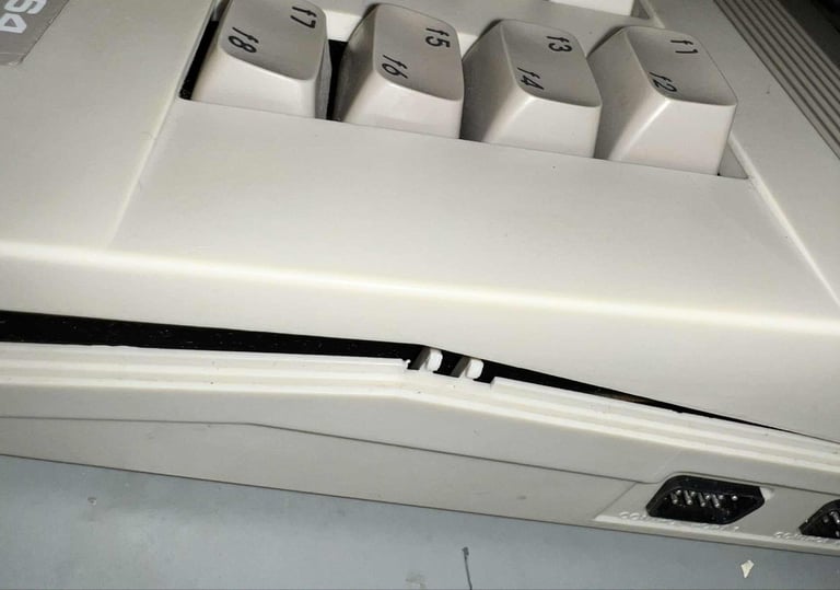
With the screws out of the way, the machine is flipped back to upright position. In contrast to the C64 breadbin, the C64C requires some finesse to disassemble to top cover from the bottom cover. Some opening pick tools are used to carefully wedge open the top cover. Note that there are two small plastic clips on both the right- and left hand side of the top cover. On the right side the clip is approximately between the F3/F5 key, and on the left side the clip is approximately between the RUN STOP/CONTROL key.

The top cover is removed and the interior is exposed. There is a substantial amount of dust and grease inside (which is to be expected since the exterior is so dirty).

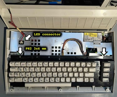
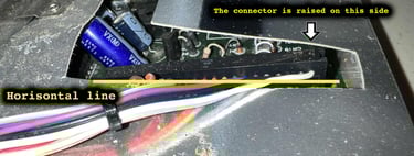
Next step is to remove the keyboard. This is mounted with two PH2 3 x 6 mm machine screws on the right- and left hand side of the keyboard. These are removed together with the LED connector. To remove the keyboard the long connector needs to be removed also. But now I notice something weird! The connector is installed skewed! How can this have happened? The machine is probably never opened before, so is this from factory?

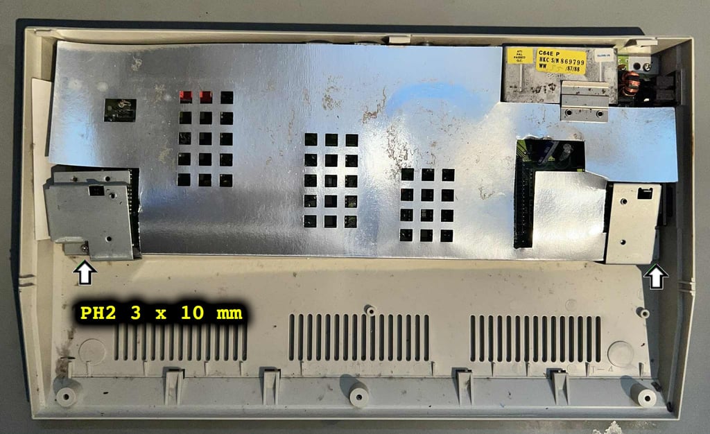
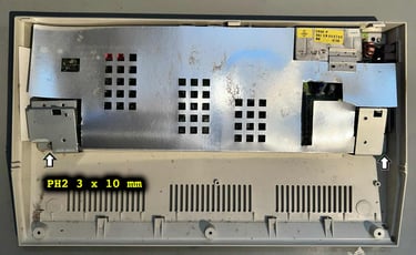
After the keyboard and LED connector are removed the next action is to remove the two screws holding the keyboard support brackets. NOTE: these screws are a bit longer than the rest of screws holding the PCB to the bottom cover. These two screws are PH2 3 x 10 mm.
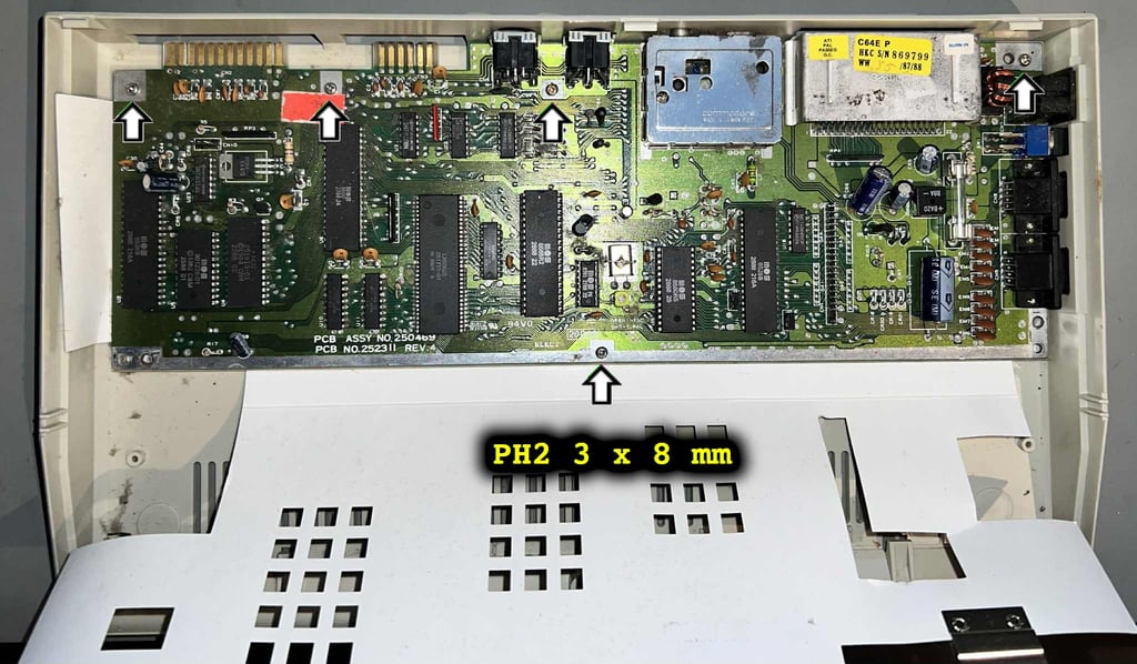
Now the RF-shield is folded away and the motherboard is revealed in all its glory. First impression is quite good. There is a SIGNIFICANT amount of dust and grime, but I can not see any immediate damage such as leakage or corrosion of any kind. The PCB is mounted to the bottom cover with five PH2 3 x 8 mm scews (note that these are shorter than the two screws holding the keyboard support brackets).

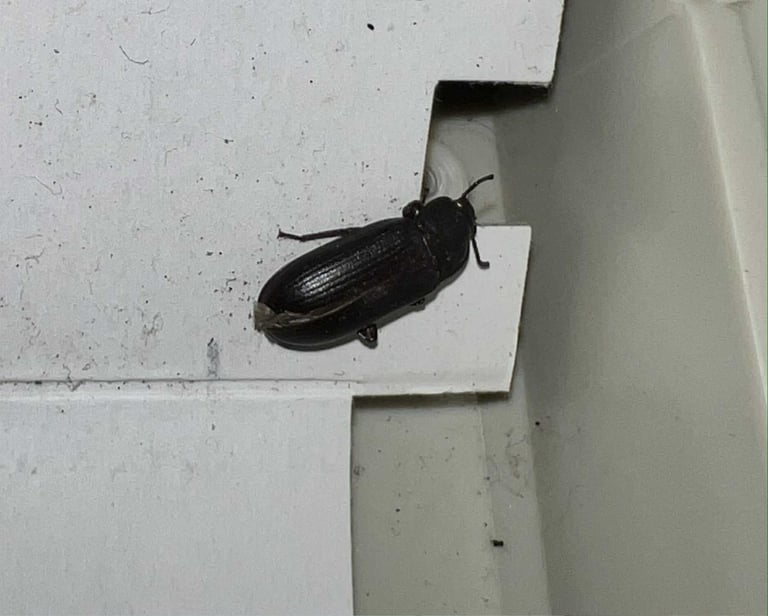
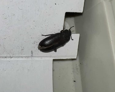
After removing the motherboard from the bottom cover a small (frightening!) surprise appears! a BUG! Holy moly! How long has this been in here?
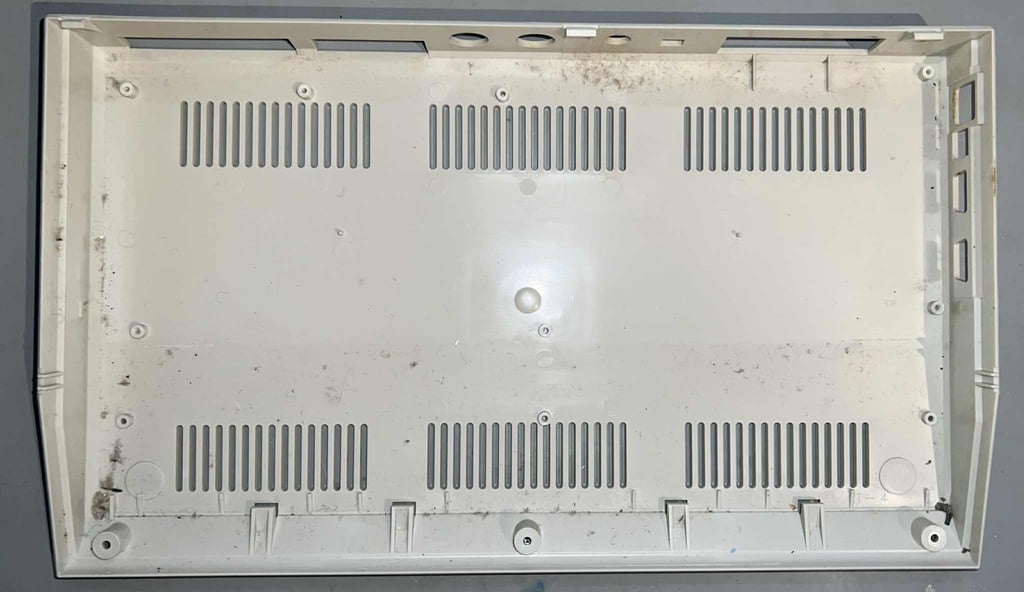
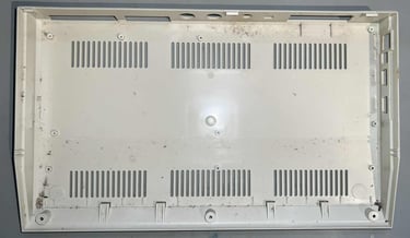
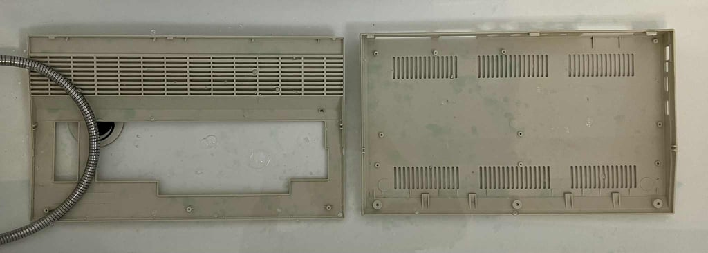
With the PCB out of the way the bottom cover is revealed. The cover is very dirty, but it does appear to be in fine condition otherwise.
Casing
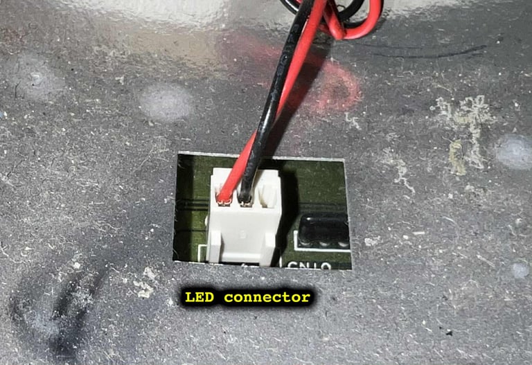
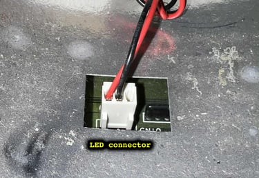
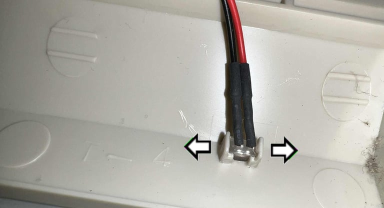
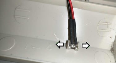
Before the top- and bottom cover are placed in a looooong bath the LED is removed. Although this is not strictly required, I think it is good practice to remove any wires since it is going to be exposed in water for a long time. The LED is quite easy to remove. Just push gently the two plastic clips away from the LED, and then carefully pull the LED out.
Since the covers are so filthy I let them soak in mild soap water for almost a week (!). This should dissolve most of the goofy stuff.

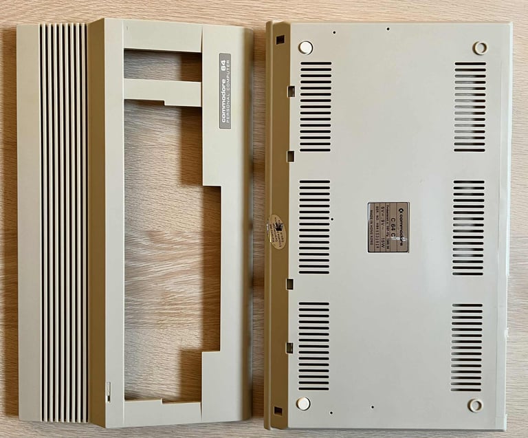
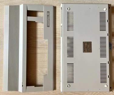
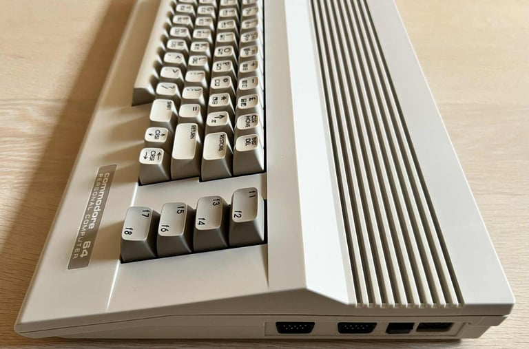
Both covers look way better after cleaning. All the grease and dirt is gone. There are some small marks still left, and the covers are slightly yellowed, but this looks so much better.

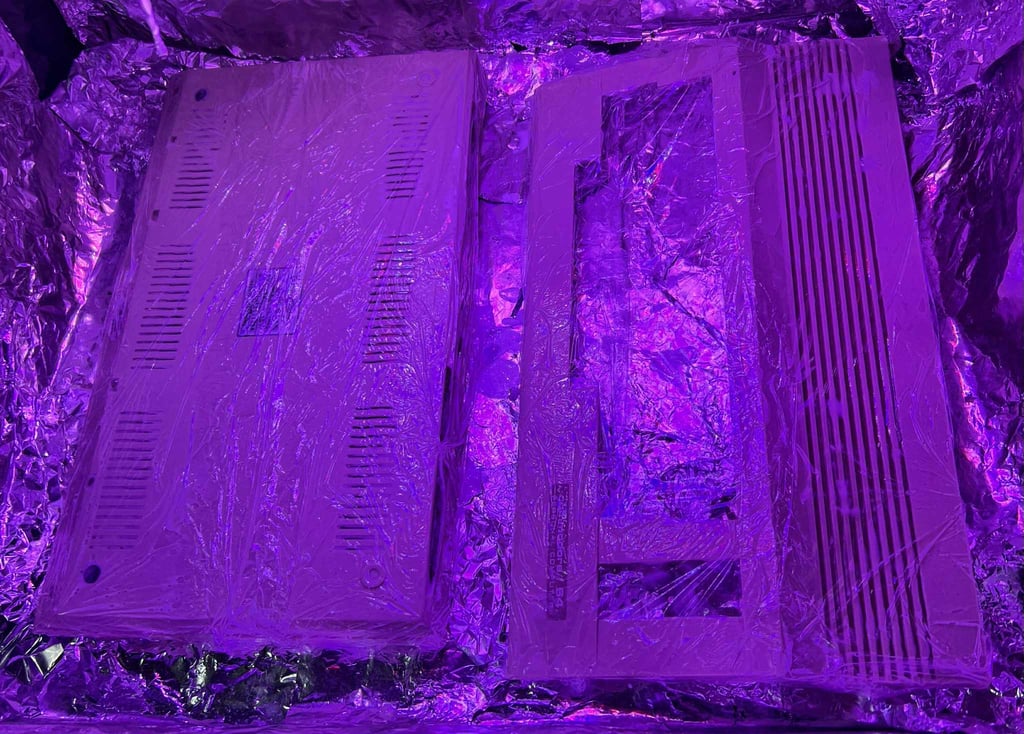
The covers are retrobrighted for about 12 hours straight. Note: before retrobrighting the bottom cover the two rubber feet are removed (otherwise they will get "sticky" during the process). Retrobrighting is done by using 12 % hydrogen peroxide cream and applying this to the covers regularly during the process. The covers are wrapped in plastic film to avoid drying out while they are exposed to UV-light in a box.

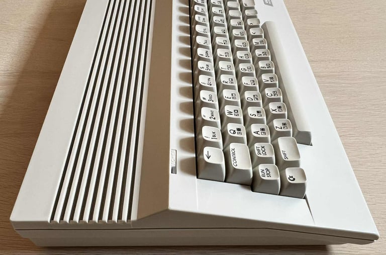
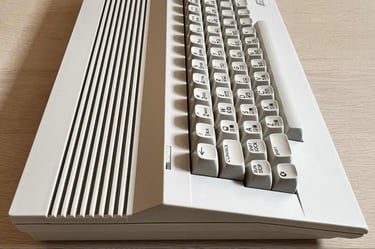
The result from the retrobrighting is very good. Not that the covers were severely yellowed, but the end result shows that most of the yellowing is now long gone.

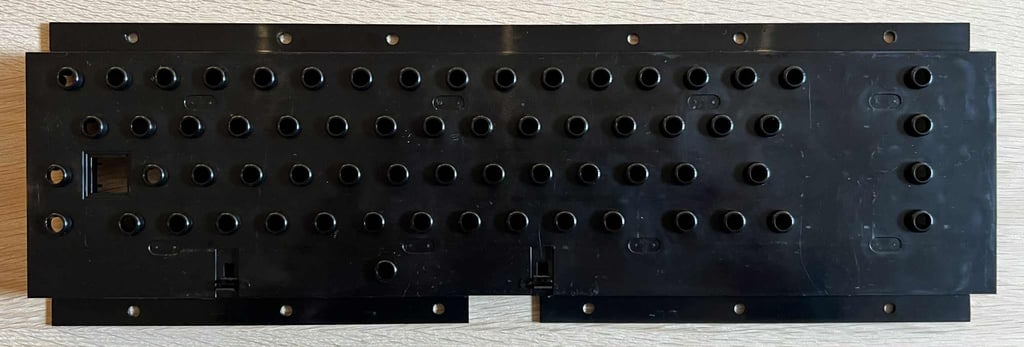
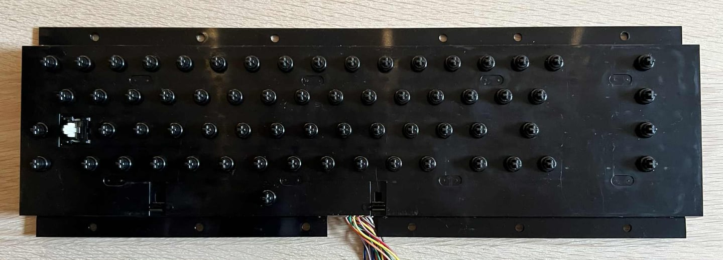
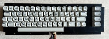
Keyboard
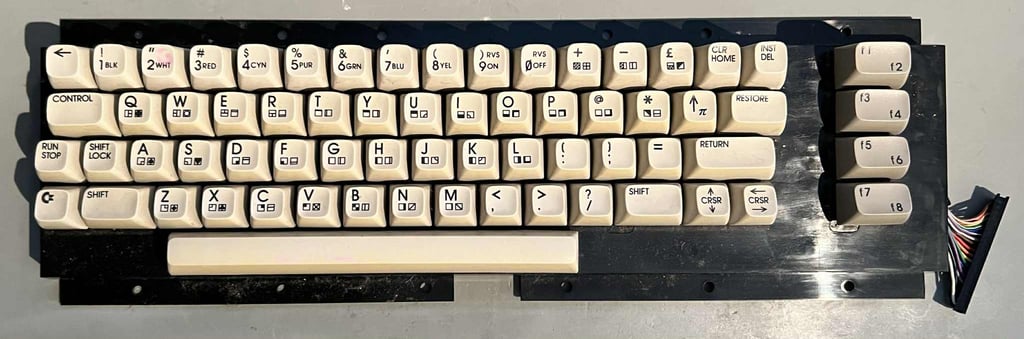
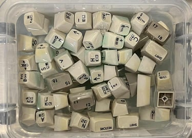
This keyboard is very dirty. All the keycaps are covered in some kind of grease, and I can see large amounts of dust and grime under the keycaps. But on the bright side the keyboard appear to be in good mechanical condition. All keycaps are nice to the touch and I can not see any damage.
All the keycaps are carefully removed with a keycap puller. Beneath each keycap there is a little spring. Note that all these springs are the same size except for the spring beneath the spacebar. So it is good practice to keep the spacebar spring in a small separate bag to avoid mixing these up.

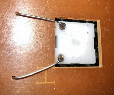
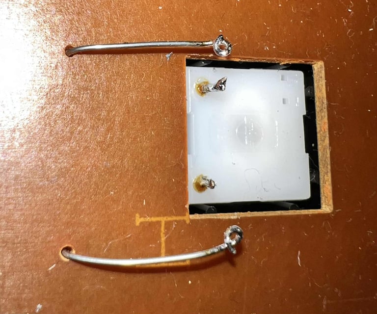
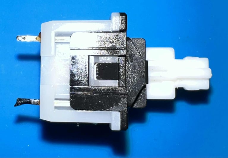
Removing the SHIFT-LOCK key is straightforward. First, the two wires on the backside are desoldered from the switch. Then the switch is pushed firmly from the backside of the keyboard towards the front side. This will make the SHIFT-LOCK switch pop out. The SHIFT-LOCK key is in good condition (after some proper cleaning with isopropanol).


All the small screws on the backside of the keyboard are removed with a PH1 screwdriver. Make sure to use a screwdriver with low torque to avoid damaging the plastic holding the screws in place.
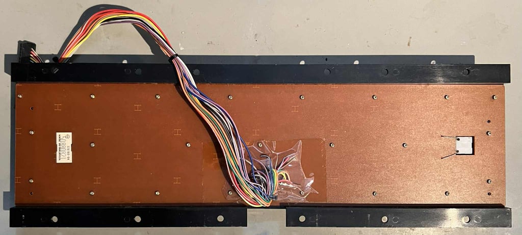

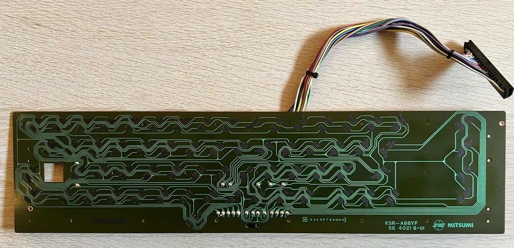
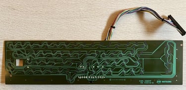
This keyboard PCB a Mitsumi KSR-A66YF 56 4021 B-01 with carbon pads. To clean the PCB only some distilled water on a paper towel is used. It is not recommended to use isopropanol on these PCS (with the carbon pads) since the isopropanol can damage the pads. The PCB seems to be in very good condition.
Next step is to clean the keycaps. This is done by placing the keycaps in a box filled with some mild soap water for a few days. This will dissolve most of the dirt and grease making them better looking, and also prepared for some retrobrighting later.

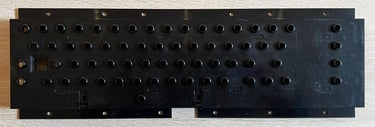
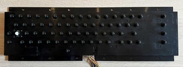
The plastic frame is cleaned with mild soap water and a soft brush. It looks as good as new after cleaning. Nice!
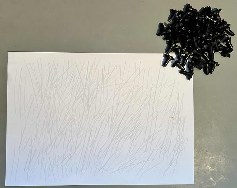
Reviving the plungers
It is very common that the plungers have accrued a thin layer of dirt on the conductive rubber. This dirt will prevent the conductive rubber to make contact with the carbon pads beneath the plunger. An effective, yet a very simple, trick is to carefull drag the plungers (the conductive rubber) over a clean sheet of paper. This will remove most of the dirt in a careful way.

And speaking of tricks. When all the plungers are revived, and are to be put back in the plastic frame, an elegant way of doing that is to lift the plastic frame with a couple of books on each side.
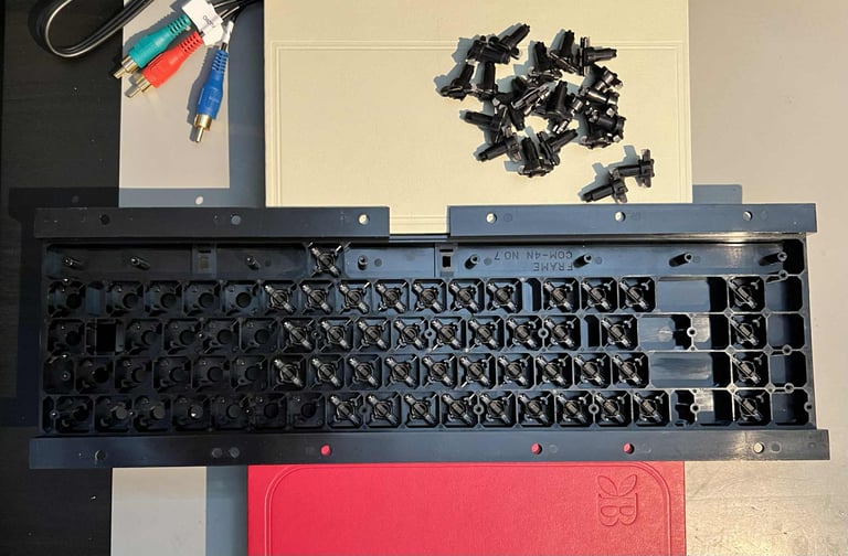

After assembling the plungers, and the SHIFT-LOCK, to the plastic frame it looks almost like new.
Retrobrighting the keycaps
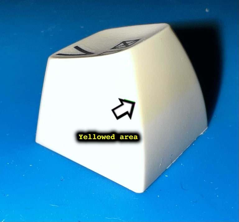
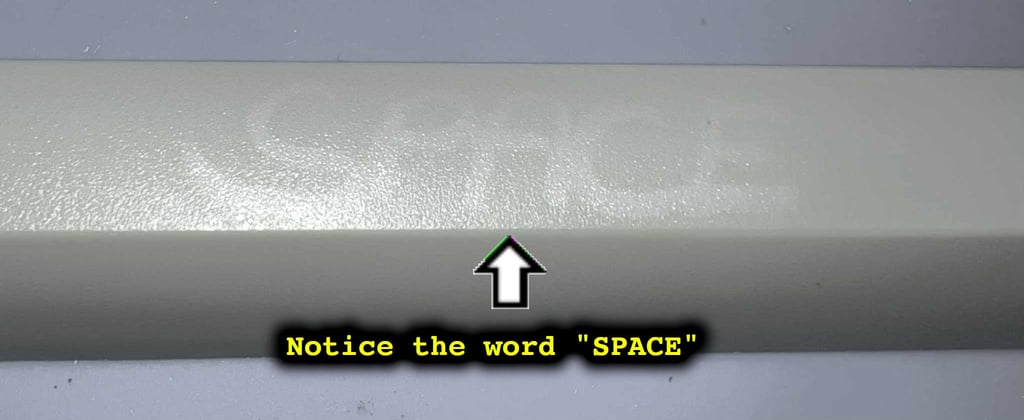
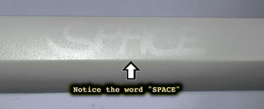
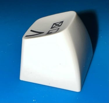
There are some slight yellowing on the keycaps. It has not gone "complete gouda", but some of the keycaps show signs of yellowing on the top of the keycaps. Also, I notice after cleaning that the word "SPACE" has been written on the spacebar (!) If I look closely on the dirty keycaps, I can see it now, but I did not notice it before cleaning. I think it is a fair assumption that someone wrote the word "SPACE" for several years ago, and also that this word was removed for a long time ago. But due to some residue from the marker pen the word still sticks due to yellowing.
Below is a picture of a keycap showing the yellowing, and a picture of the spacebar (with fake colours to show the word "SPACE" better).

For a better retrobrighting result (and also to ease the operation) all the keycaps are placed on a 3D printed plastic bracket.

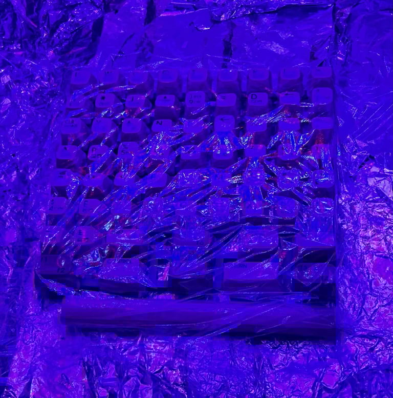
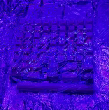
12 % hydrogen peroxide cream is "painted" on all the keycaps. The keycaps are "painted" with this cream regularly during the 12 h period where the keycaps are exposed to UV light in a box. Note that some cling plastic film are covering the keycaps during the whole period to avoid the cream from drying.
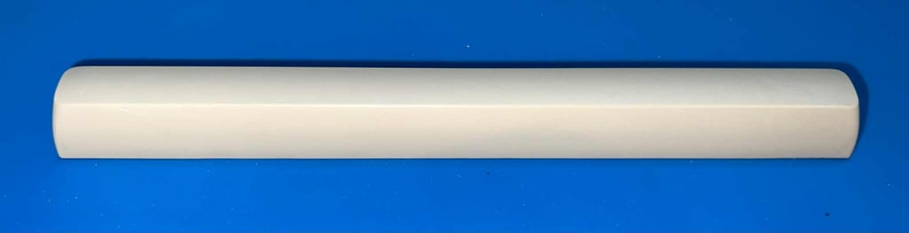
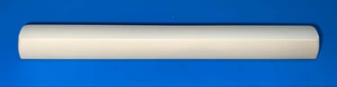
The result after retrobrighting is very good. Most of the yellowing is gone. Below are some pictures of the "V"- and "SPACEBAR" key after retrobrighting. As far as I can see the word "SPACE" is gone (!)

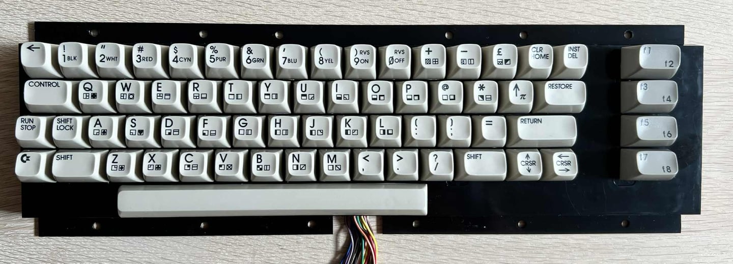
All the keycaps are mounted back to the keyboard. Looks good as new!
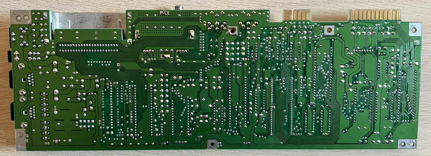
Mainboard
Visual inspection
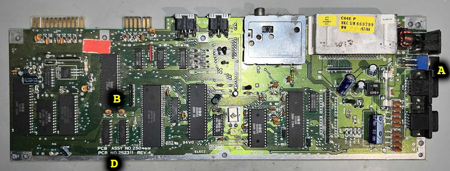
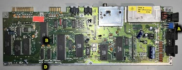
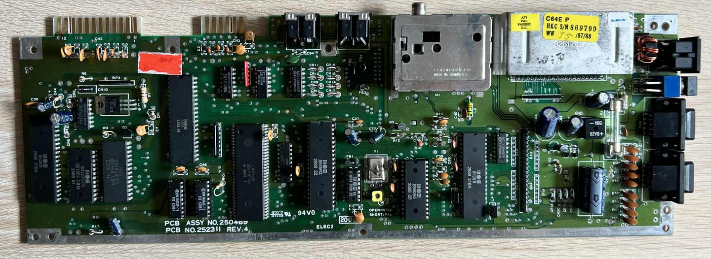
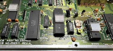
This is an Assy 250469 mainboard 252311 Rev 4 mainboard. The mainboard looks to be in quite good condition, but it is incredibly dirty. Doing a visual inspection this is what I notice:
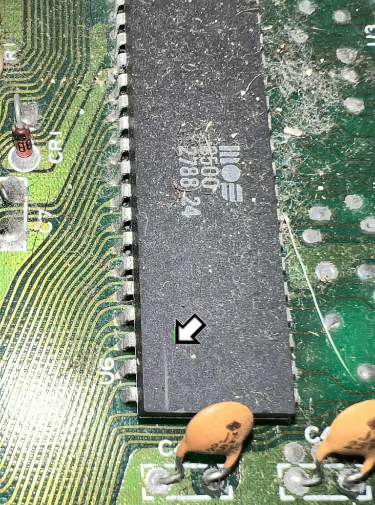
A: There is a small scratch on the left bottom side of the MOS 8500 CPU IC. It is really marginal, but nevertheless worth checking.
B: The switch is completely stuck in "ON" position.
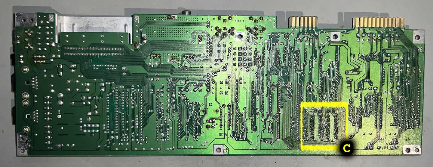
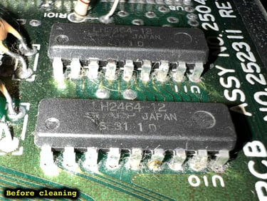
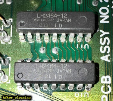
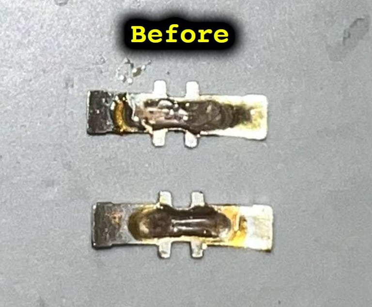
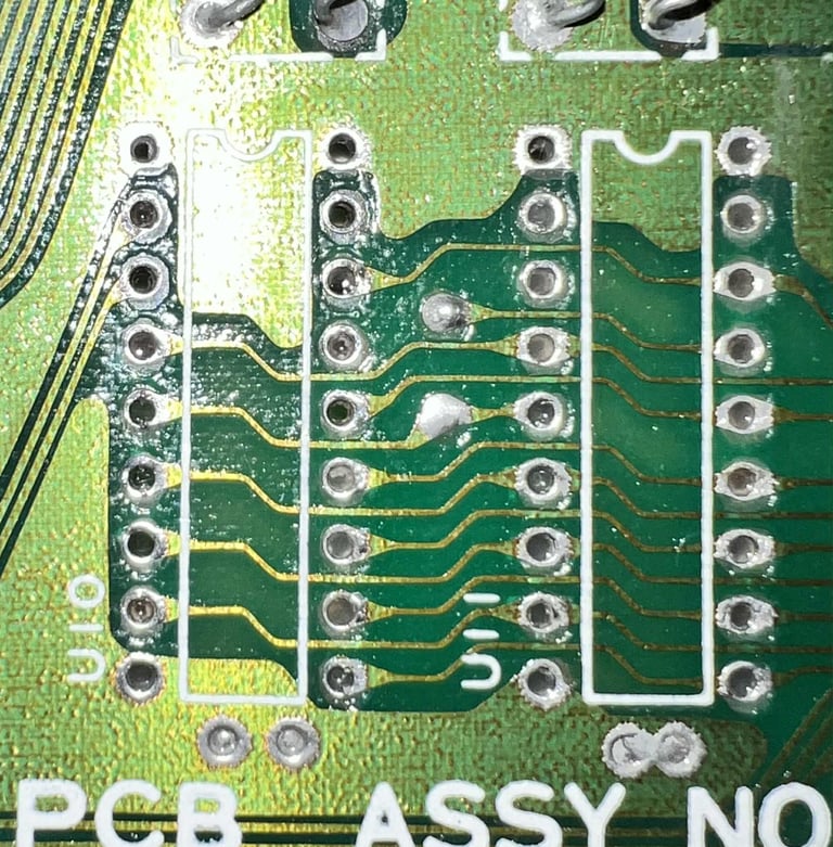
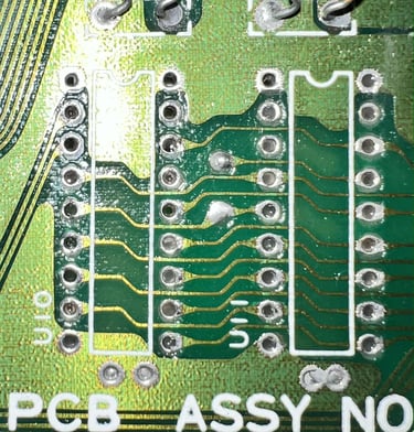
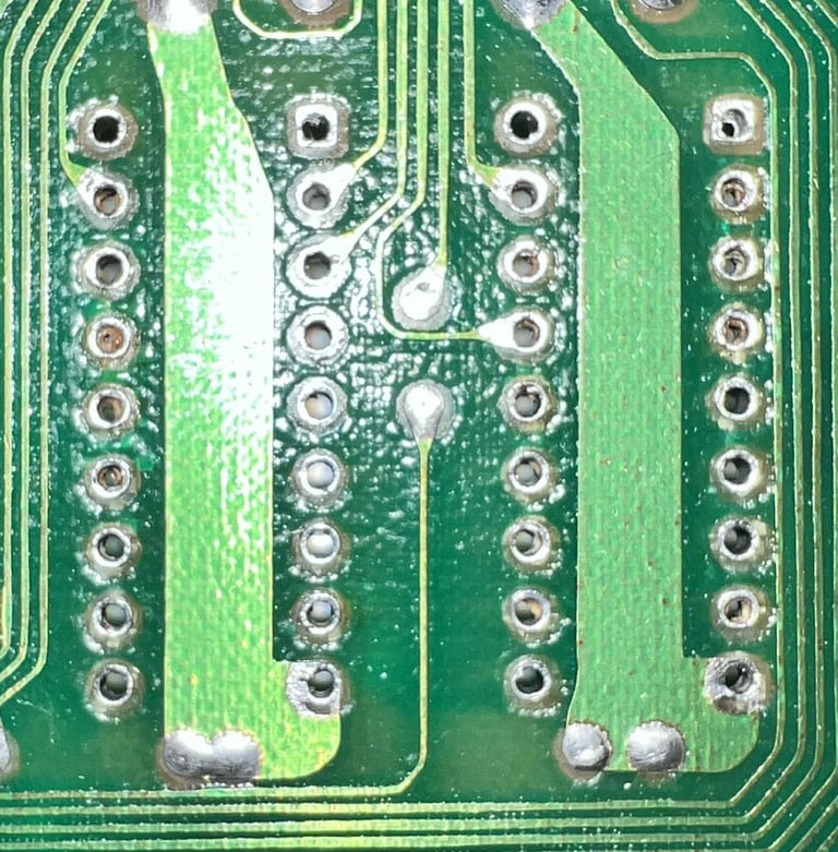
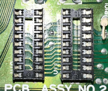
C: There are quite some flux residue on the backside of the mainboard - especially around the RAM ICs (U10 and U11). UPDATE: In this area there are also signs of corrosion.
D: The pins on the RAM ICs are not very well soldered - some of the pins have hardly any solder on the top side of the mainboard (U10 and U11).

Some close-up pictures of the CPU scratch and the RAM ICs (before and after a quick clean) are shown below.


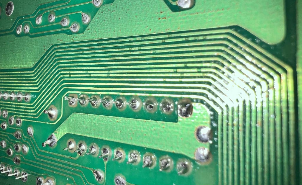
Also, in the area next to the left RAM IC (will be on the right hand side when seen from the underside of the PCB) there are signs of corrosion of several of the traces. These traces are connecting some of the pins of the MOS 8500 CPU to other ICs on the board. The corrosion seems to be not very serious, but it needs to be looked into.

In the table below all the custom ICs are listed. And as can be seen from this table is that all original ICs were produced between week 27 to week 31 of 1988 so I think we can assume that this Commodore 64C was produced in the late summer/autumn of 1988. Could very well be that the first owner of this machine was listening to "Sweet Child o´mine" from Guns N´Roses while playing Last Ninja 2!
Initial testing
An initial test is performed on the mainboard. This is done with the purpose of checking the initial status of the mainboard - checking for any fault symptoms. In the table below the result are shown.
Cleaning the mainboard
Before the repair, and refurbish, continues the mainboard is cleaned. This is done by first removing the socketed ICs (and the fuse), and then washing the mainboard with mild soap water and a paint brush. After cleaning the mainboard is left for drying for a couple of days. Below are some pictures of the mainboard after cleaning.

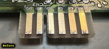
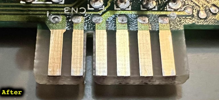
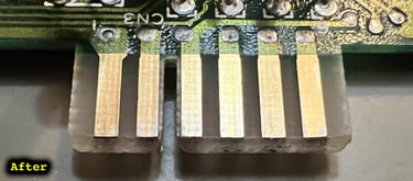
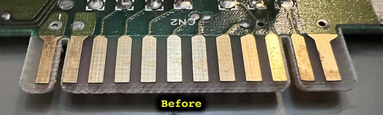
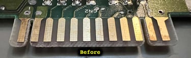
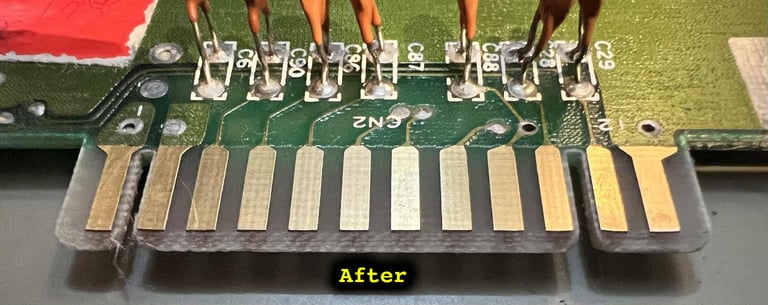
Cleaning the User (CN2)- and datasette (CN3) port
The user- and datasette port are not very oxidised, but there is still a need to revive the gold plated connectors. To clean the connectors a combination of an old school rubber eraser and isopropanol is used . See pictures below.


Checking the voltages
For the Commodore 64 to work flawlessly all the different voltages need to present and within acceptable tolerances. A detailed article on the subject can be found in the HOWTO - Checking the C64 voltages. In the table below all the measures voltages are listed (this list will also be updated after refurbishment). All the required voltages are present and within tolerances, so there are nothing obvious wrong in that area.
Mainboard - Repair
Observations - cartridges
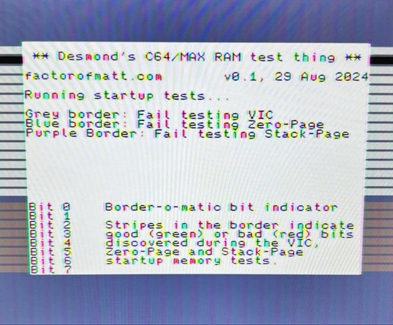
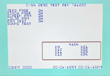
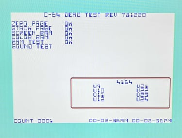
Both the Dead Test- and the DesTestMax cartridge indicates a RAM fault. But I do not think that is the fault. The reason for that is based on the following observations:
The Dead Test cartridge does not give a solid fault indication. It changes between one and six flashes. As there are only two RAM chips on this board the flashes would indicate a fault in both RAM ICs (according to the Dead Test manual). Although not impossible, I do not think it is likely.
The DesTestMax fails promptly at the initial stage. If it was a "real" RAM fault I would expect that only some of the bits very faulty.
Observations - oscilloscope
Probing around the mainboard a first possible clue is found:
With no test cartridge installed: All data lines D0-D7 are stuck "HIGH". There are some small fluctuations, but not so much that the lines are pulled "LOW". See picture below.

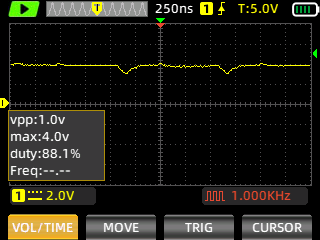
But we do know that the C64C did show some signs of life with the Dead Test- and DesTestMax cartridge(?) And probing the same D0-D7 when either of these cartridges are installed there are activity on all of these datalines! Probing both the address- and datalines with an oscilloscope shows activity. So in short, there does not seem to be any data- or address line stuck HIGH/LOW/FLOATING.
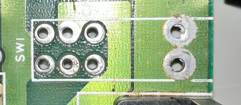
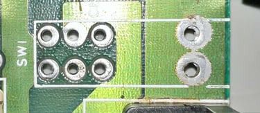
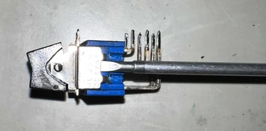
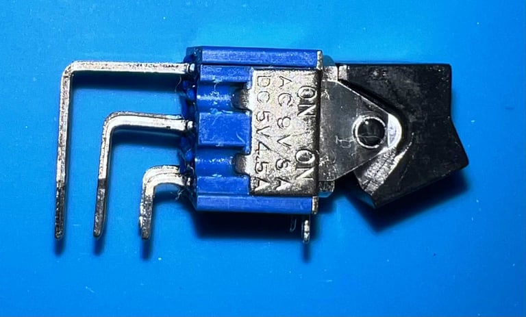
Repairing the power switch (SW1)
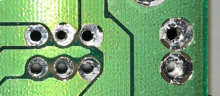
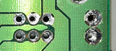
Before continuing the probing for any fault indicator the power switch is repaired. Luckily, the power switch (SW1) on the Commodore 64 can often be repaired. It is quite common for these to get stuck after many years sitting still in a storage room. To repair the power switch it needs to be desoldered first. When desoldering the power switch notice that it is wise to add some fresh solder to the solder points first. The six input/output pins are easily desoldered at 330 degrees Celcius, but the two additional pins used to mount the switch requires about 370 degrees (and using both the soldering iron and desoldering gun).
No traces or pads were damaged during desoldering.
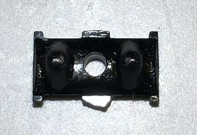
Opening the power switch is not trivial, but not impossible. The first step is to carefully pry open the two side plates holding the top part fastened to the rest of the switch.
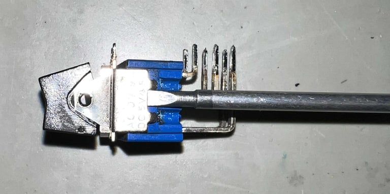
When removing the top part be careful not to loose any of the tiny parts inside the switch. With a pair of precision tweezers the two small metal plates are removed. And as can be seen from the pictures below these are incredible dirty. There is some sticky "goo" on these which would cause poor contact. The metal plates are cleaned with isopropanol and contact cleaner.
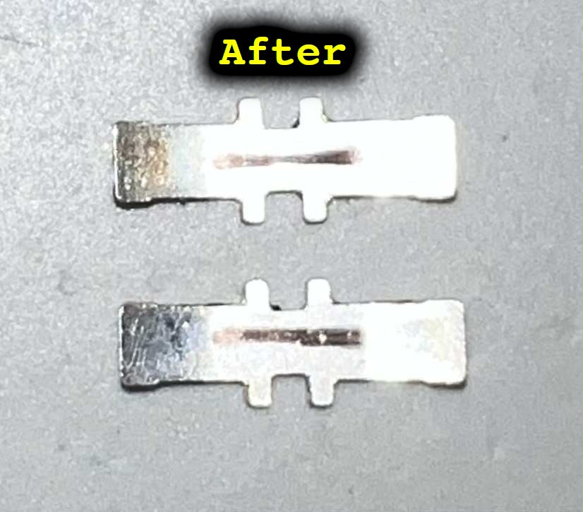
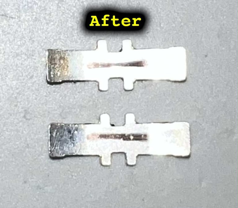
Also, there is a tiny little plastic parts which is used as the "rocker" in the switch. This is cleaned with some isopropanol. Notice that there is a small part which appears to be broken off. But I do not think this will matter anything for the switch to function.

Assembling the switch can be a fiddly due to the small parts, but with some patience the power switch is put back together. The six legs are also cleaned with a brass pen and isopropanol. Good as new (!)

Looking for the fault(s)
I am still sceptical that there is actually something wrong with the RAM IC. I can´t rule it out, but the reason why I do not think that it is the RAM ICs are based on the following:
The DesTestMax copies 4k of data from $F000 - $FFFF to $3800. This is for the VIC-II to use, but from my point of view this is also a sign that the RAM is at least partly working. I am able to see the DesTestMax startup screen so the RAM can not be completely dead.
The Dead Test shows both 1 or 6 flashes. And according to the Dead Test manual that should indicate a fault in U10 or U11, but why is the fault not consistent.
The DesTestMax shows that the first RAM fault is found at address $0002 and ALL bits are bad.
So, at face value, the cartridges are indicating the both U10 and U11 are both bad. It is not impossible, but I think it is unlikely.
After several hours of checking for bad traces and weird signals, I really can´t find anything. All data- and address lines looks fine, reset- and clock lines are OK and I can not find any broken trace anywhere.
My guess is that the fault is either:
In one, or both, of the RAM ICs
In the MOS 8500 CPU
In the Super PLA
Checking the RAM ICs
Even if I think this is a red herring I choose to check the RAM ICs first. Both ICs are desoldered from the board. When I desolder on the board I use both a solder iron and a desoldering gun. The solder iron is held at the top of the board pins, and the desolder gun is held at the bottom side (330 degrees Celcius). No traces or pads are damaged, but I really do think that these are in not the best condition. They look a bit dull and grey, but they are working as they should. The pads are cleaned with a glassfiber pen and isopropanol.

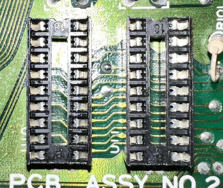
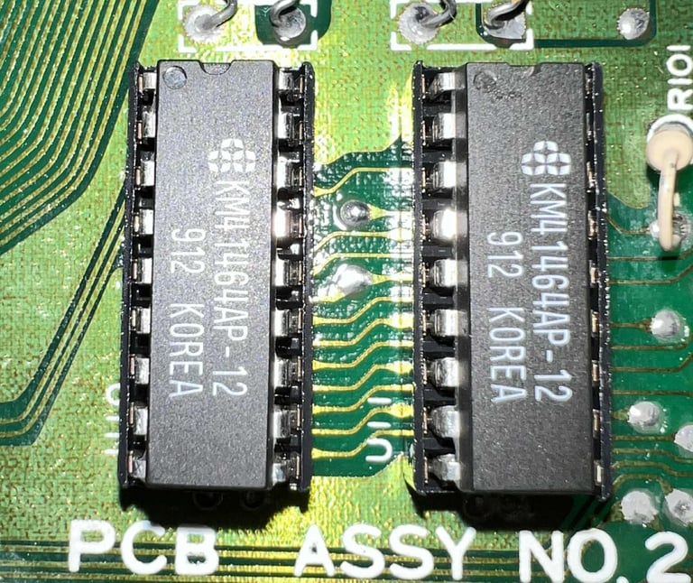
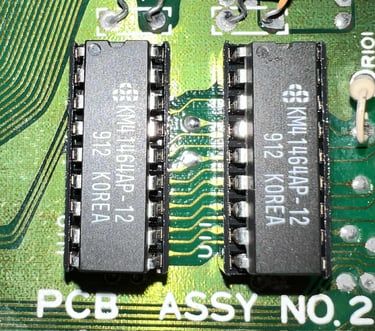
Two new dual wipe sockets are installed, and 2 x KM4146AP-12 RAM ICs (from Samsung) are installed.
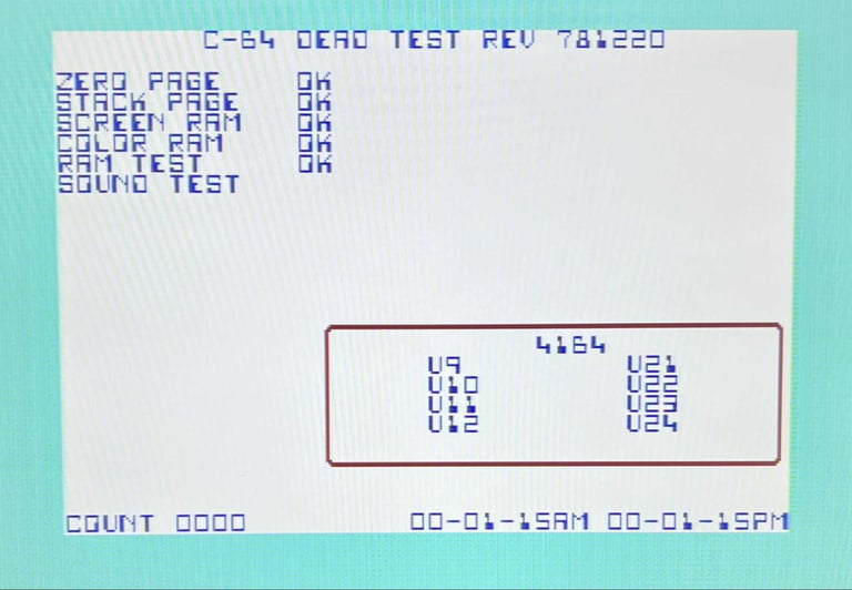
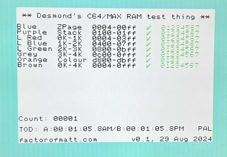
So, the big question: does the installation of new RAM ICs solve the problem? Well.... partly! With the new RAM ICs the status is now shown in the table below.
Both the old RAM ICs turns out to be bad - so my hypothesis that it was not the RAM ICs was not correct. Now the machine runs the Dead Test and DesTestMax cartridge which is a good point for further diagnostics. See below for some pictures, and a video, from the test described above.

Chasing the next fault
My guess is that the next fault is caused by a bad ROM IC: the combined Kernal/BASIC MOS 251913-01. This is based on the following clues:
The machine is now "working" with the Dead Test and DesTestMax cartridge. These cartridges does not require any of the ROM ICs to be functional.
Both the DeadTest and DesTestMax gives an indication that the CIA #1 and #2 are ok. Although this is not a proper test of these the TimeOfDay (TOD) seems to be working just fine which is an indication that these are fine.
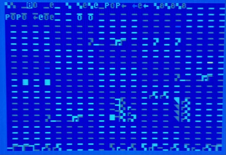
The times when the machine boots (?) to the garbled screen the PETSCII characters are OK. That means that the data stored in the Character ROM (MOS 901225-01) seems to be fine.
The garbled screen is reacting (affecting the scrolling) when knocking on both the Kernal/BASIC and Character ROM
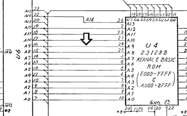
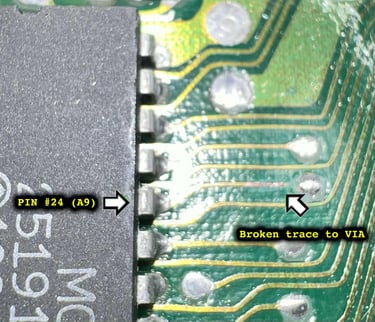
Before desoldering an IC it is good practice to always check all connections first. And when doing that I notice that there is a broken trace between PIN #24 (on the Kernal/BASIC ROM) and PIN #16 (on the CPU). And since this trace is address line A9 this is a crucial problem. Could this be the cause of the fault?

By close inspection I can see that there is a broken trace between PIN #24 on the ROM IC and to the nearest VIA.

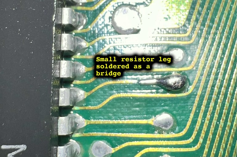
The area surrounding the VIA is first neutralised with some vinegar. Then the area is cleaned with isopropanol, and the VIA and part of the trace is scraped clear for both oxidation and silk screen. This will make the repair easier as the solder has something to adhere to. Some fresh solder is applied to both the exposed trace and the VIA, and a small piece of a resistor leg is used to bridge the gap.

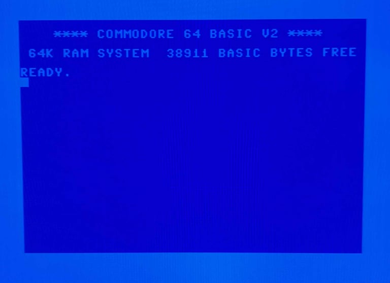
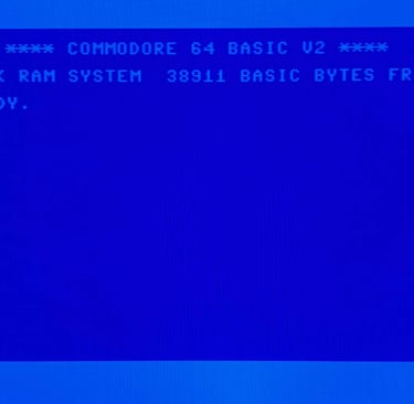
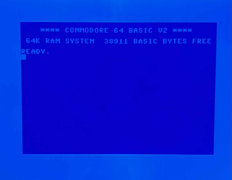
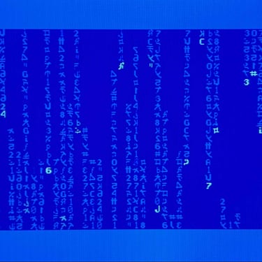
Does this fix the problem? Yes! When powering on the machine the famous blue screen with 38911 BASIC BYTES FREE appear. See table below for status.
Below are some pictures of the mainboard after cleaning and repair. NOTE: I have stopped re-capping Commodore 64s just for the sake of re-capping. Why? My experience (and many others in the retro Commodore 64 community) the re-capping of a Commodore 64 is very seldom necessary. There are cases where capacitors dry out, but this is very rare indeed (compared to other machines such as Amigas SMD capacitors).

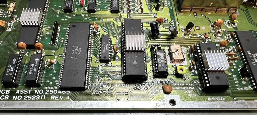
Adding heat sinks
Some of the custom MOS chips can run quite hot. And as a mean to protect these chips heat sinks are added to these. A small heat sink is added to the SID-, VICII-, and CPU chip. Note that I do not use large heat sinks covering all the chip. You could argue that this could improve things, but I think it is actually sufficient to cover only the center of the chip - this is where the chip logic is actually located and the heat generated.
Testing
Proof is in the pudding - does it work?
Testing is done through three main stages:
Testing the basic functionality and chips
Testing the complete set of custom ICs and I/O ports
Testing by using the machine playing demos, games etc. accessed by both floppy and datasette to verify correct operation
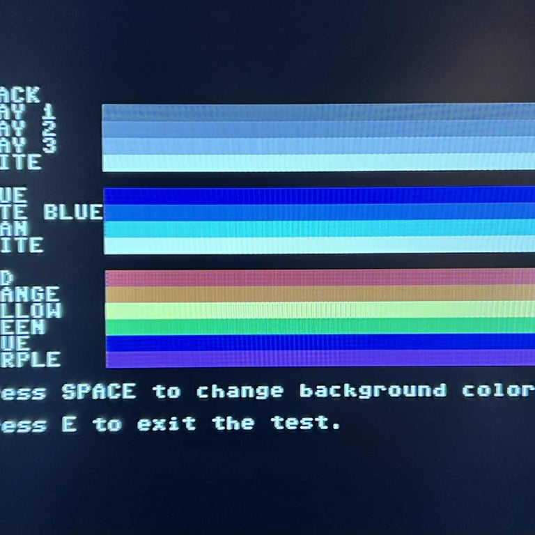
NOTE: Some of the colours are "off" due to a poor LCD monitor used for the pictures. All colours are correct, but they do not appear correct in the pictures.
Basic functionality and chips
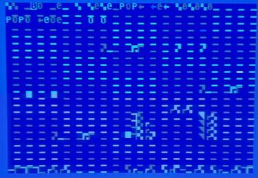
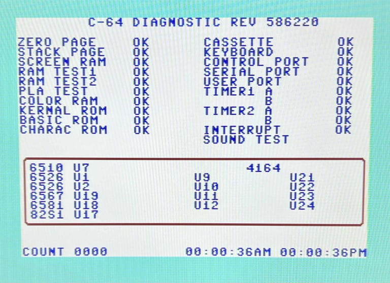
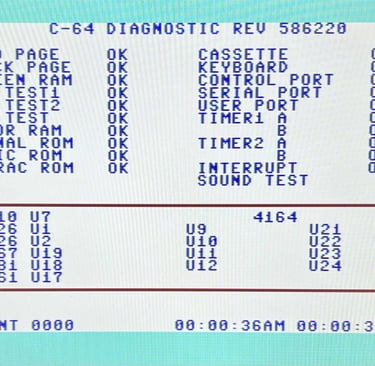
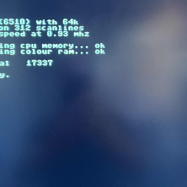
First test is done using the Dead Test Cartridge. This test doesn´t test all the functionality of the Commodore 64, but it does test the basic functionality of the major chips such as the CIA #1/2, CPU, VIC-II, PLA, RAM and SID. As the picture shows below the test is passed.

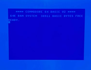
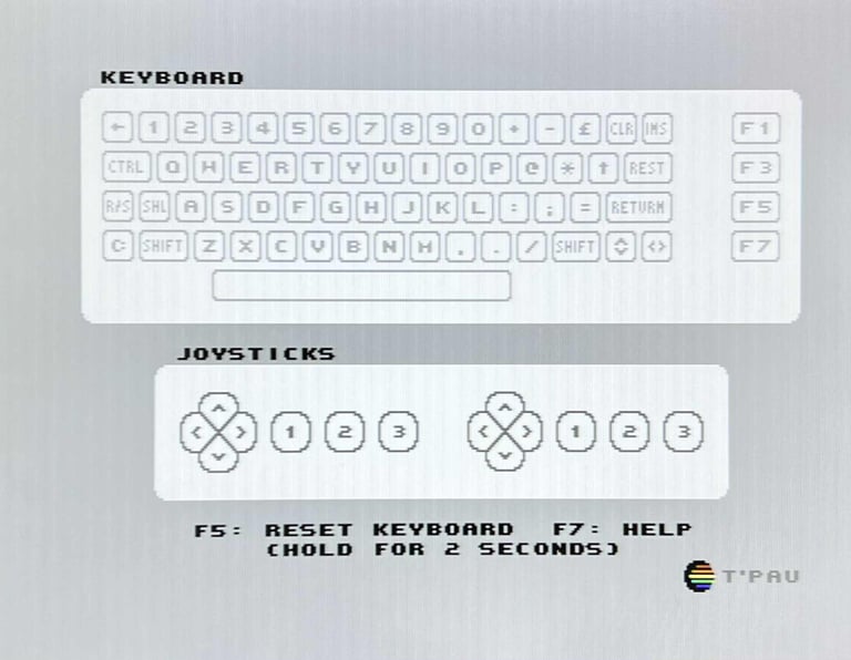
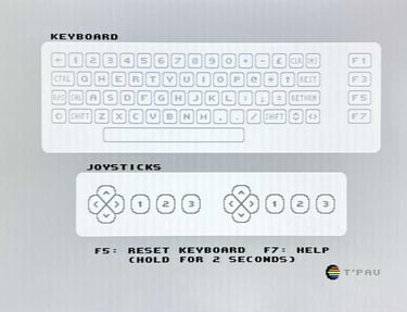
Next test is to power the Commodore 64 to the blue boot up screen and also check the keyboard to make sure all keys works as they should. The test is passed; all keys works and 38911 BASIC Bytes Free.
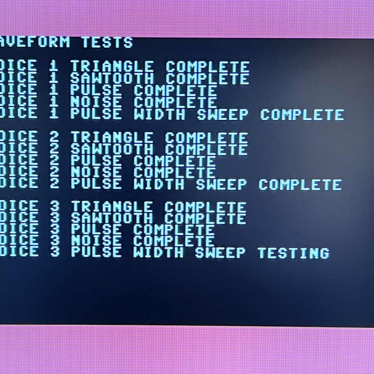
The basic functions of the VIC-II, SID and RAM is tested with 64 Doctor, Commodore 64 SID tester and MemTest64. Note that this is to be considered as basic functionality - more advanced (?) functionality such as sprite handling / collision detection / advanced audio will be tested later.
Diagnostics test with harness
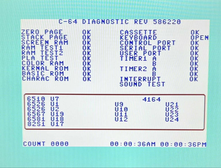
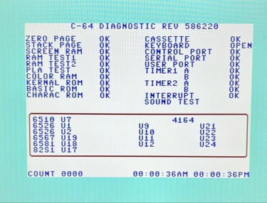
To test all the custom ICs, and I/O ports, the Diagnostics cartridge is used. The Diagnostics cartridge is very valuable when the complete test harness i installed as in "everything" is tested formally. As can be seen from the picture below, no issues are identified.
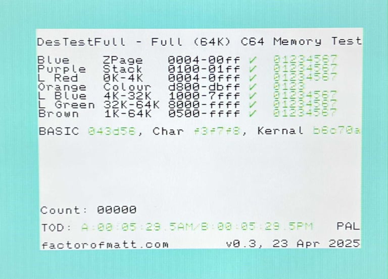
Testing the full 64k of RAM
To make sure that all the 64k of RAM is fully working the DesTestFull cartridge is used. This software use the March-B algorithm to test all the RAM extensively. No issues are identified.

Extended testing
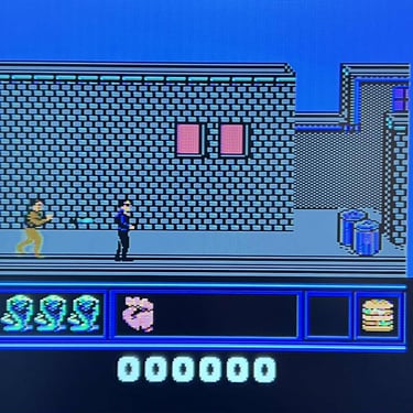
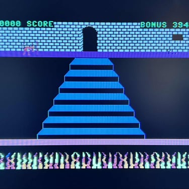
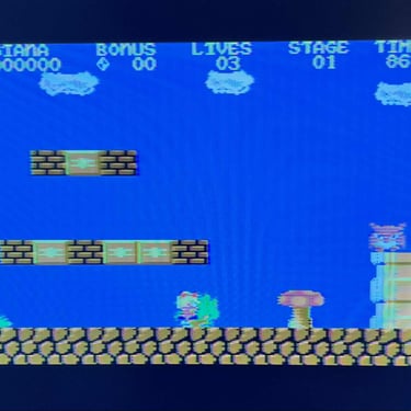
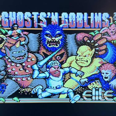
Knowing that the basic functionality of the machine works I continue the testing by using the Commodore 64 for normal operations; playing some games, watching demos, loading from datasette and floppy and using a cartridge. I can not find any issues with this machine. I also pay special attention to the video to make sure that there are no glitches in the graphics - I can´t see any abnormalities. Below is a gallery with pictures from the testing.


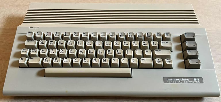
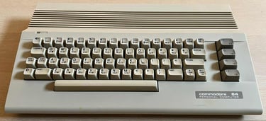
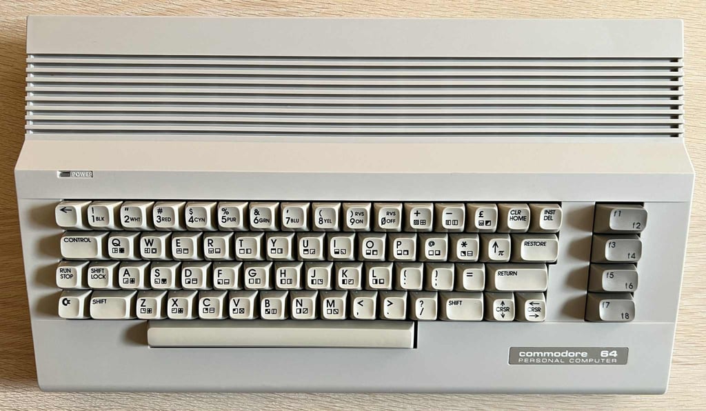
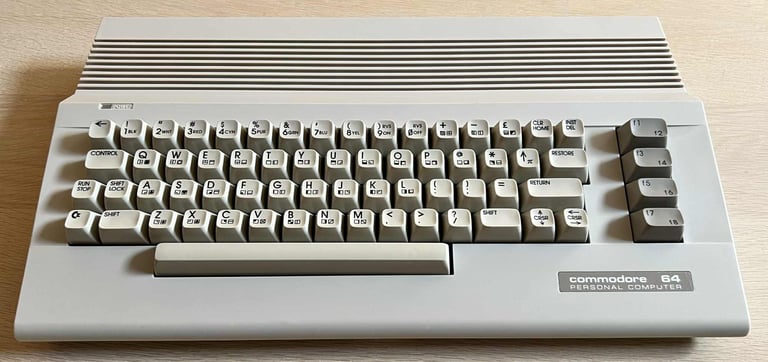
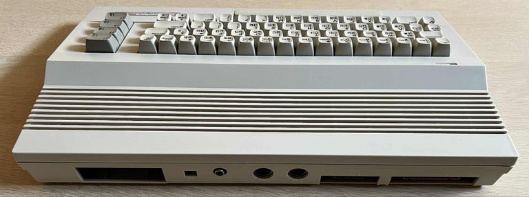
Final result
"A picture worth a thousand words"
Below is a collection of the final result from the refurbishment of this C64C. Hope you like it! Click to enlarge!

