

Signal reference
CPU
MOS 6510
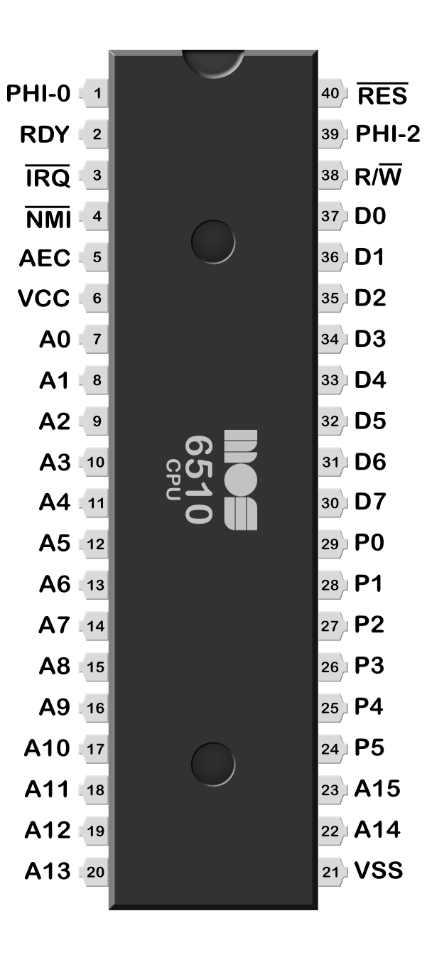
Pinout
Reference signals
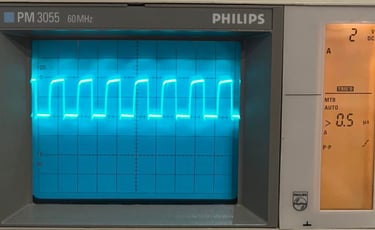
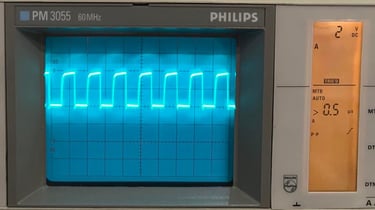
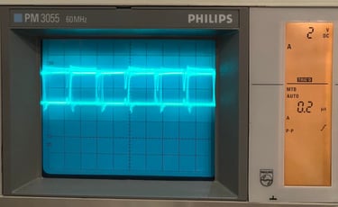
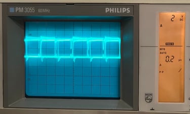
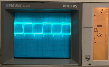
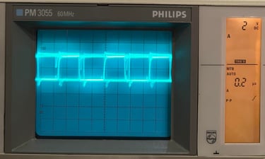
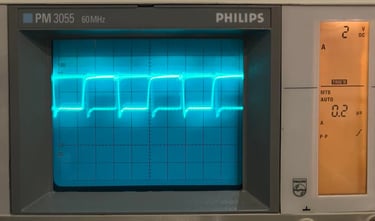
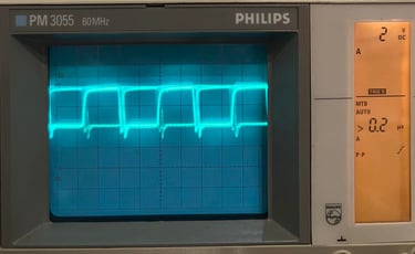
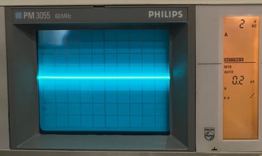
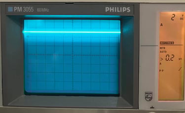
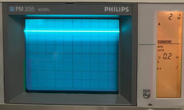
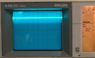
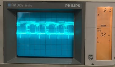
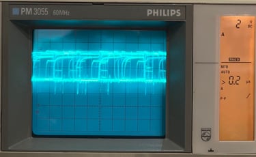
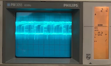
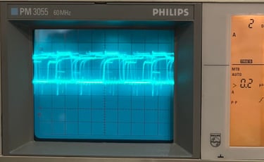
Below are simple pictures of the different signals on the CPU MOS 6510 chip which I use for reference/comparison during fault finding. For further details about the signals on the different C64 custom chips I will highly recommend Sven´s techsite. Information about the pinout is taken from: https://ist.uwaterloo.ca/~schepers/MJK/6510.html
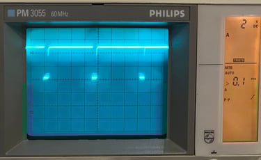
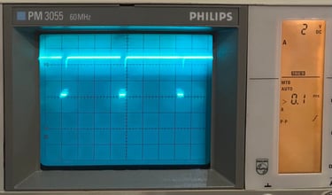
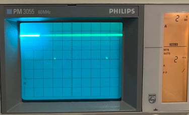
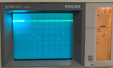
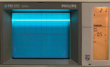
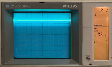
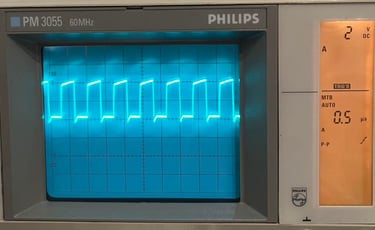
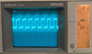
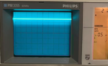
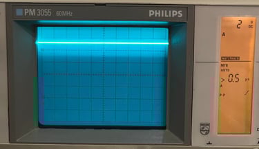
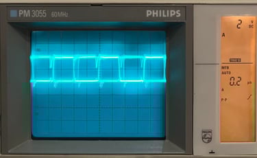
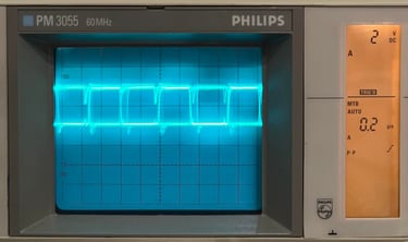
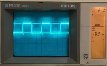
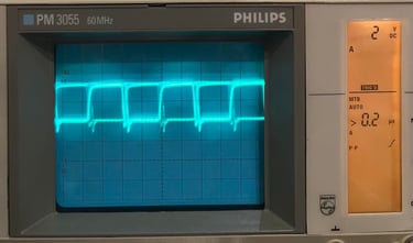
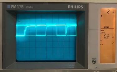
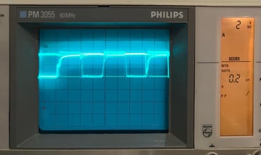
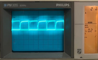
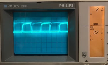
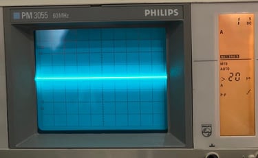
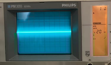
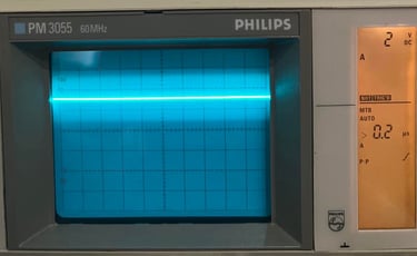
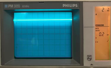
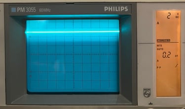
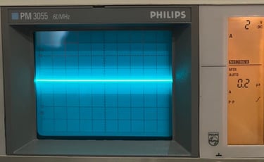
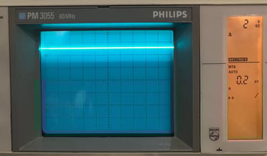
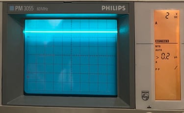
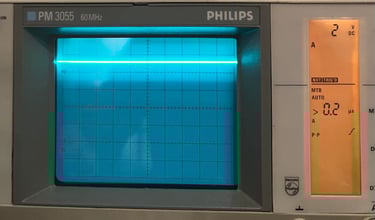
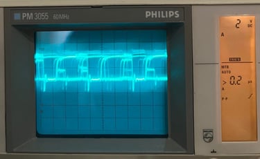
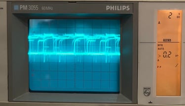
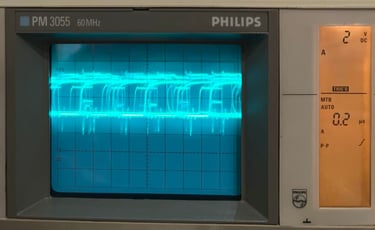
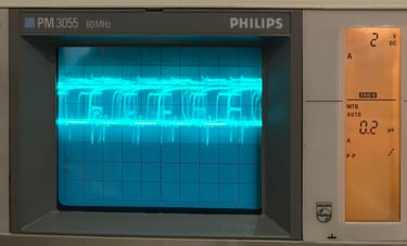
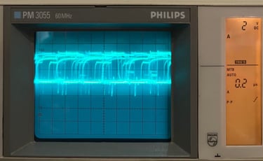
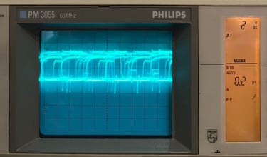
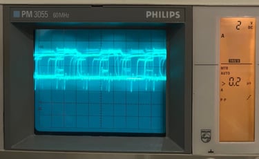
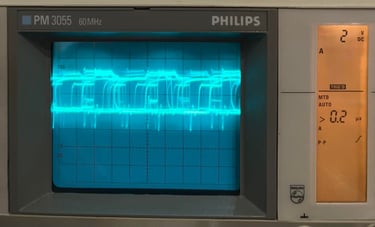
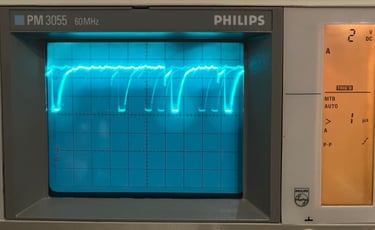
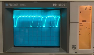
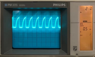
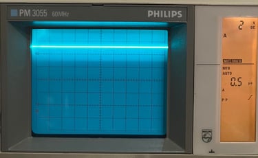
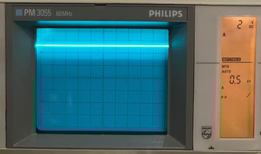
Settings on Philips/Fluke PM3055 60 MHz analog oscilloscope:
2 V / DIV
See individual pictures for time settings
Signals have been measured on a working Commodore 64 assy 250466 in idle mode (blue screen).
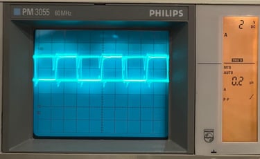
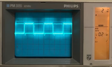
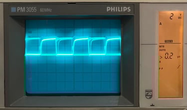
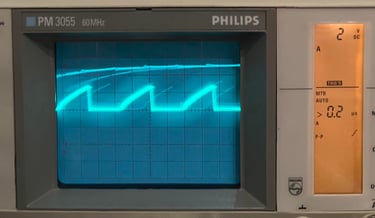
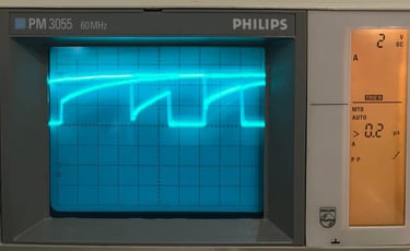
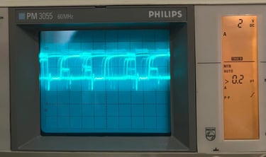
Pin #1
ø 0 in
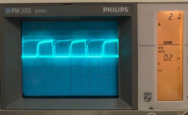
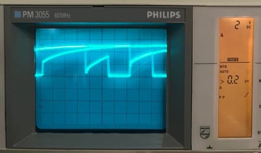
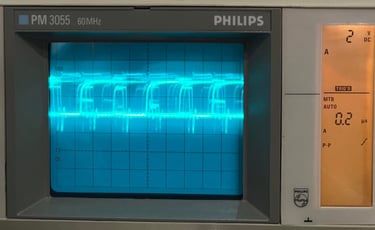
Pin #2
RDY
ReaDY. When going LOW, the CPU waits after next read cycle for this line going HIGH again.
The RDY signal the result of logical AND between BA and DMA produced by the chip U27 (74LS08).
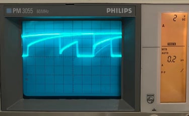
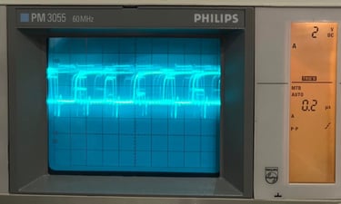
Pin #3
/IRQ
Interrupt ReQuest. When going LOW, the CPU loads the PC with the value stored in $FFFE / $FFFF after processing the current command. This procedure will be executed only when interrupts have been enabled (bit 2 in flag register = 0). Note that the IRQ signal must be applied until the CPU has checked this pin; a short IRQ pulse is not sufficient.
In the C64, there are three possible sources for an IRQ: VIC-II [PIN8] , CIA #1 (timer)
Expansion port [PIN4]
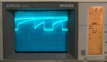
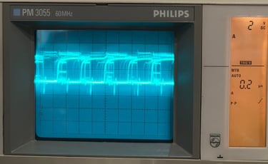
Pin #4
/NMI
Non Maskable Interrupt. When going LOW, the CPU loads the PC with the value stored in $FFFA / $FFFB after processing the current command. In the C64, there are three possible sources for an NMI:
- RESTORE key
- CIA #2
- Expansion port, pin D
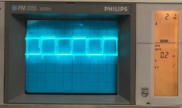
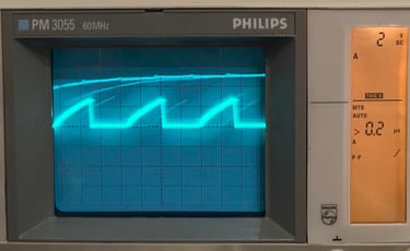
Pin #5
AEC
Address Enable Control. When going LOW, the CPU puts the address bus into a 'tri-state' (hi impedance) mode and is thus totally decoupled from the rest of the system, so that another chip can take control over it. This means that other systems or processors can use the Commodore 64 circuitry - e.g. when transferring data to and from a disk drive or another computer.
Phi 0 in. The system clock signal, which is generated by the VIC-II in the C64, is applied to this input. In the C64, it is about 1MHz.
Pin #6
VCC
Supply voltage. This pin is connected to +5V DC.
Pin #7
A0
Addressline A0
Pin #8
A1
Addressline A1
Pin #9
A2
Addressline A2
Pin #10
A3
Addressline A3
Pin #11
A4
Addressline A4
Pin #12
A5
Addressline A5
Pin #13
A6
Addressline A6
Pin #14
A7
Addressline A7
Pin #15
A8
Addressline A8
Pin #16
A9
Addressline A9
Pin #17
A10
Addressline A10
Pin #18
A11
Addressline A11
Pin #19
A12
Addressline A12
Pin #20
A13
Addressline A13

Pin #21
VSS/GND
GrouND.
Pin #22
A14
Addressline A14
Pin #23
A15
Addressline A15

Pin #24
P5
(Peripheral I/O port)
Unique to 6510 vs 6502
Connected to datasette port C/3 (indirect). This pin mirrors the value of bit #4 stored in memory address $0001. DEFAULT: On power-on bit #4 is "1" ($0001).
Pin #25
P4
(Peripheral I/O port)
Unique to 6510 vs 6502
Connected to datasette port F/6 (indirect). This pin mirrors the value of bit #4 stored in memory address $0001. DEFAULT: On power-on bit #4 is "1" ($0001).
Pin #26
P3
(Peripheral I/O port)
Unique to 6510 vs 6502
Connected to datasette port E/5 (indirect). This pin mirrors the value of bit #3 stored in memory address $0001. DEFAULT: On power-on bit #3 is "0" ($0001).
Pin #27
P2
(Peripheral I/O port)
Unique to 6510 vs 6502
Output which is connected to /CHAREN on PLA. This control signal determines whether the 2332A 4K character generator ROM (U5) or the I/O devices are within the address space $D000-$DFFF. When CHAREN is logic LOW, addressing a location anywhere within $D000-$DFFF will access the character generator ROM. The 6510 CPU access this ROM when copying the character set from ROM into RAM. DEFAULT: This pin is HIGH disabling the character ROM and enabling the I/O devices.
Pin #28
P1
(Peripheral I/O port)
Unique to 6510 vs 6502
This output is connected to /HIRAM on PLA and is used to bank the 2364A 8K operating system Kernal ROM (U4) in or out of address space $E000-$FFFF. If HIRAM is at a logic LOW, address space $E000-$FFFF is part of the RAM memory. DEFAULT: This pin is HIGH enabling Kernal ROM.
Pin #29
P0
(Peripheral I/O port)
Unique to 6510 vs 6502
Databus line D7
Pin #30
D7
This output is connected to /LORAM on PLA. The LORAM signal from P0 determines whether the 2364A 8K BASIC ROM (U3) or an 8K section of RAM is part of the CPU´s $A000-$BFFF address space. LORAM at logic LOW causes the RAM to be in address $A000-$BFFF. DEFAULT: This pin is HIGH enabling BASIC ROM.
Pin #31
D6
Databus line D6
Pin #32
D5
Databus line D4
Pin #33
D4
Databus line D5
Pin #34
D3
Databus line D3
Pin #35
D2
Databus line D2
Pin #36
D1
Databus line D1
Pin #37
D0
Databus line D0
Pin #38
R /W
Read/-Write. With this line, the CPU controls whether the next DRAM access will be a read or write cycle. LOW=write, HIGH=read. Or in other words; controls the direction in which data moves on the D0-D7 bits of the data bus. Note that all accesses only take place when ø2 is HIGH.
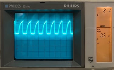
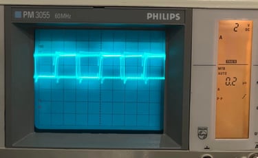
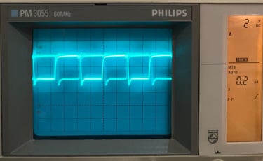
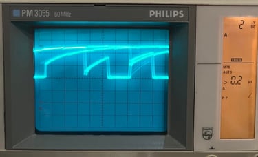
Pin #39
ø2 out
Phi 2 out. The CPU outputs the system clock for the rest of the chips for synchronization. The 6510 CPU produces the inverse of of Phi 0 -> a 0.985248 MHz (PAL) Phi 2 system clock signal. The frequency is 1.02 MHz in NTSC mode.
Pin #40
/RES
RESet. When going LOW, the CPU resets and waits for a LOW-HIGH transistion to load the PC with the value stored in $FFFC/$FFFD. After power-up, timer A in the NE556 in the C64 pulls this line to LOW for a short time and half a second later back to HIGH.
Banner picture credits: Xato