

Signal reference
VIC-II
MOS 6569
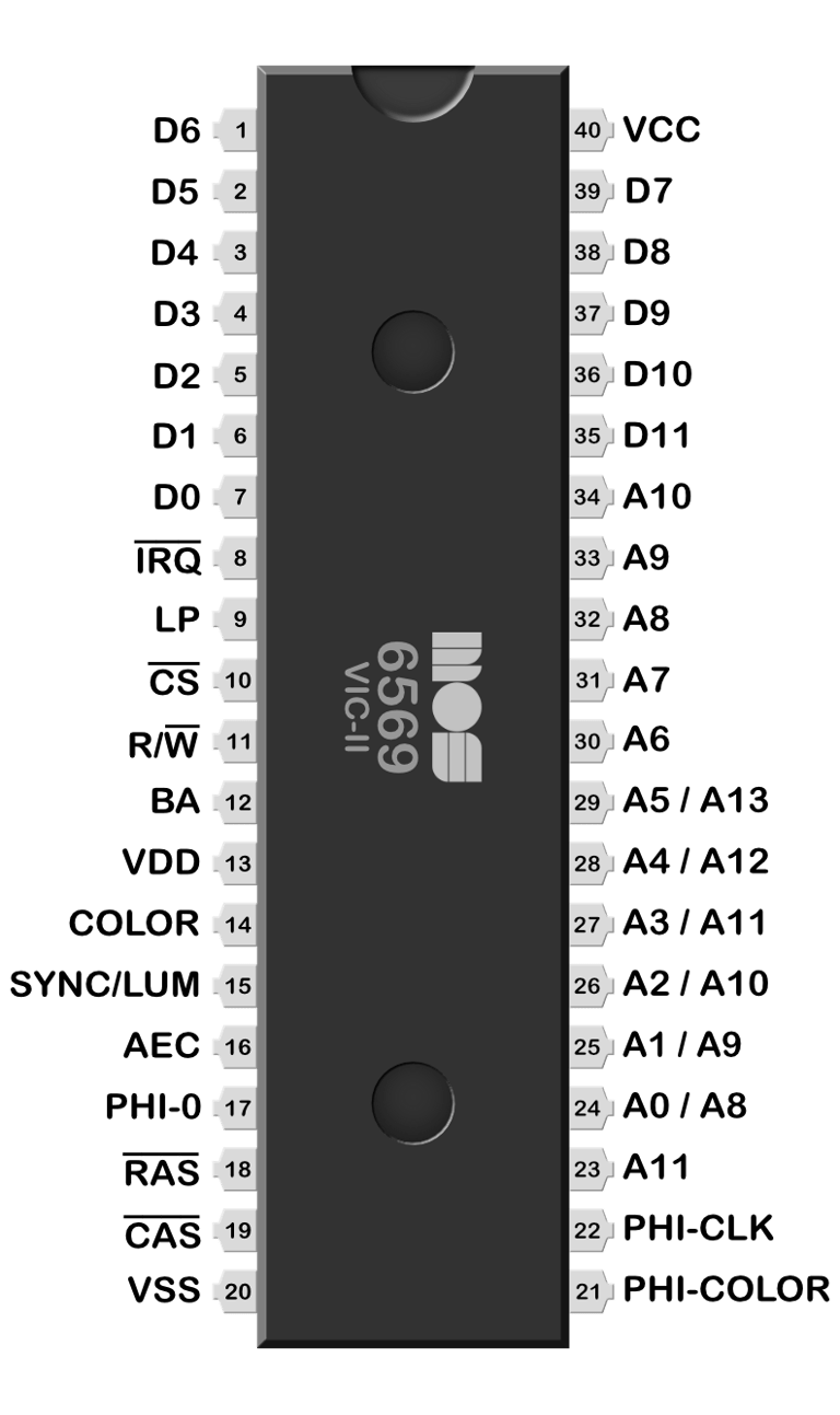
Pinout
Image credits: Commodore Repair Toolbox (https://github.com/HovKlan-DH/Commodore-Repair-Toolbox)
Reference signals
Below are simple pictures of the different signals on the CPU MOS 6569R5 chip which I use for reference/comparison during fault finding. For further details about the signals on the different C64 custom chips I will highly recommend Sven´s techsite. Also there is a magnificent article about the VIC-II by Christian Bauer which I highly recommend if you are interested in learning the inner details of the VIC-II chip (http://www.zimmers.net/cbmpics/cbm/c64/vic-ii.txt).
Information about the pinout is taken from:
https://ist.uwaterloo.ca/~schepers/MJK/vic2.html and https://en.wikipedia.org/wiki/MOS_Technology_VIC-II
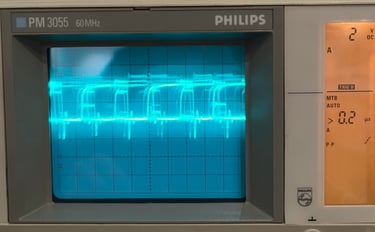
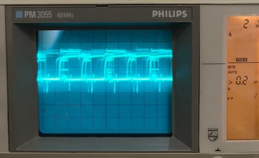
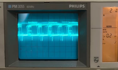
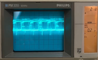
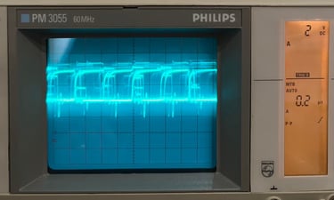
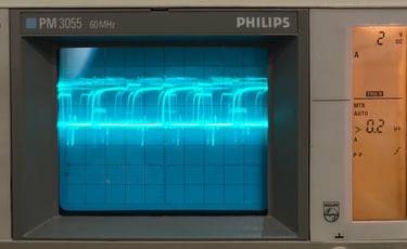
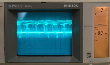
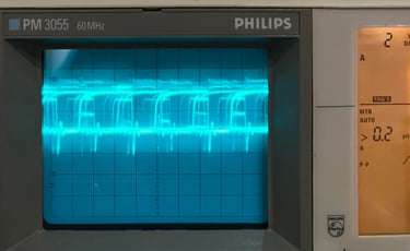
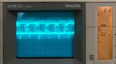
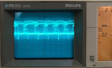
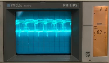
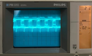
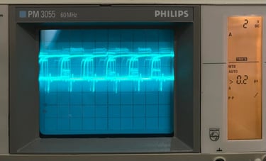
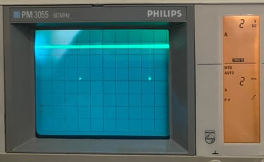
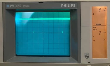
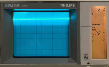
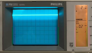
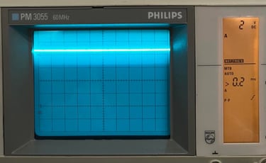
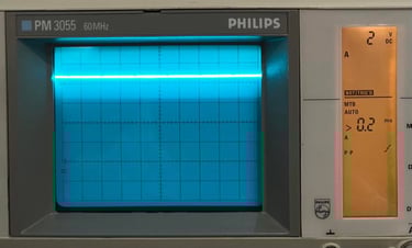
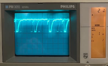
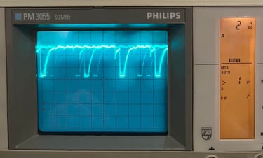
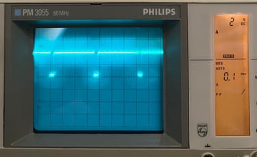
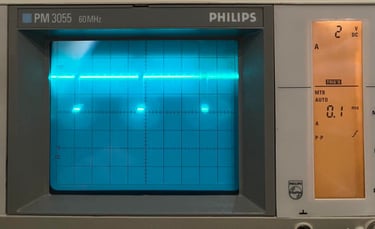
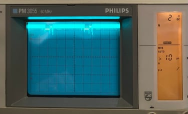
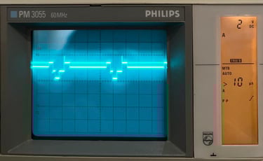
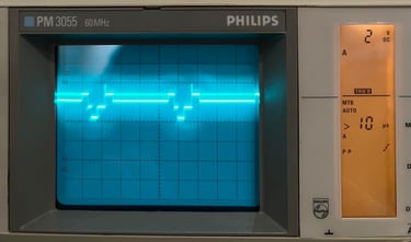
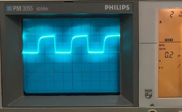
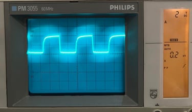
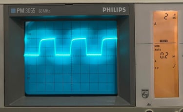
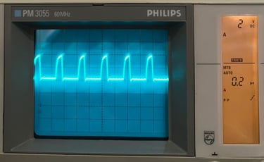
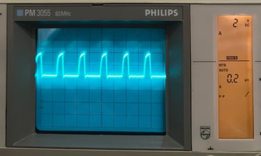
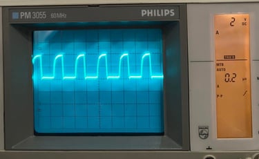
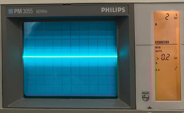
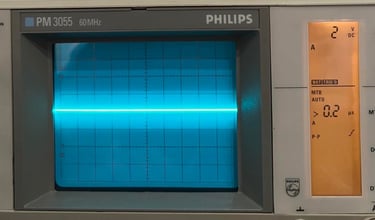
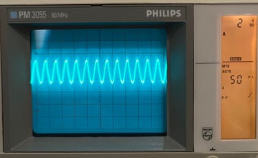
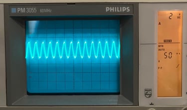
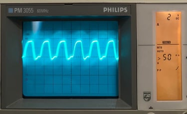
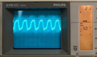
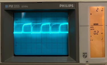
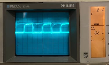
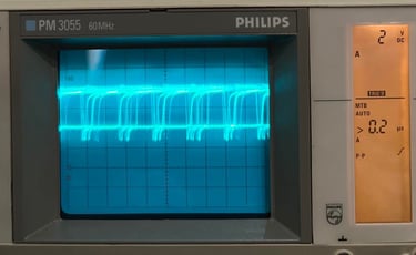
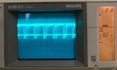
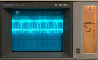
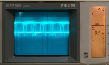
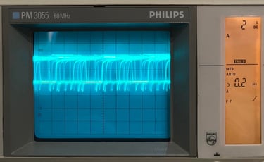
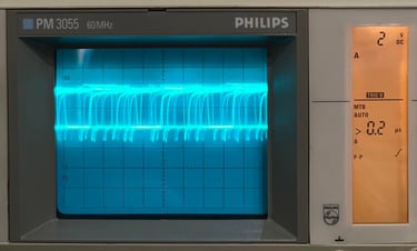
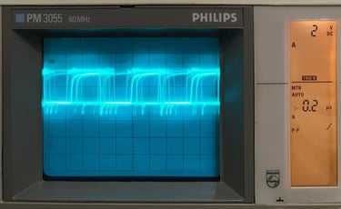
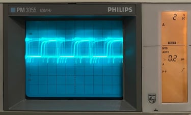
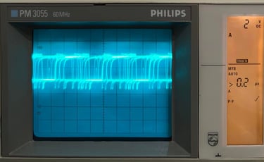
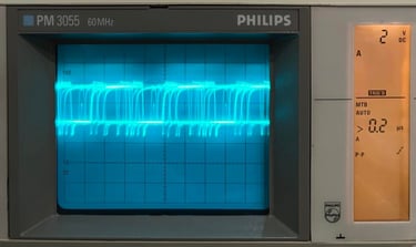
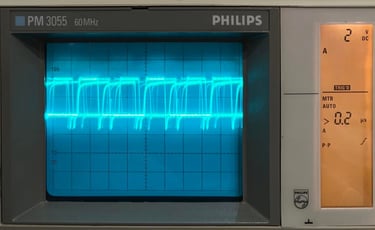
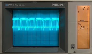
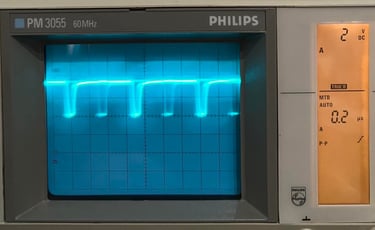
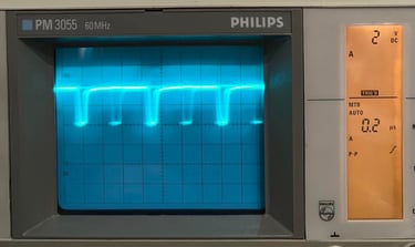
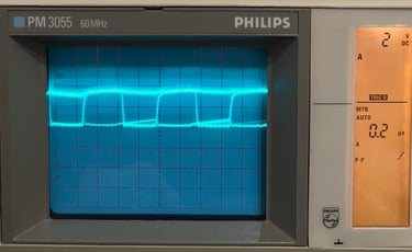
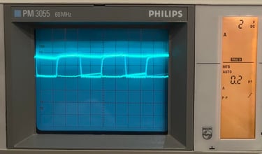
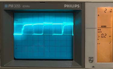
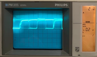
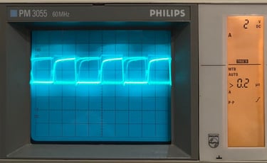
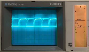
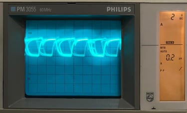
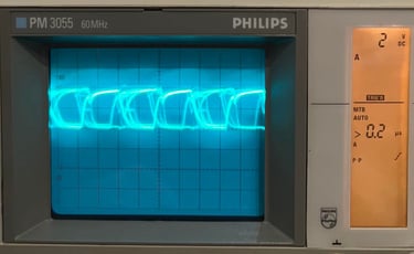
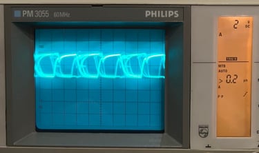
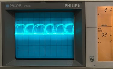
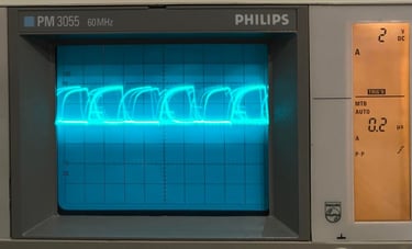
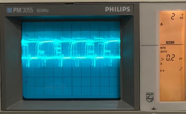
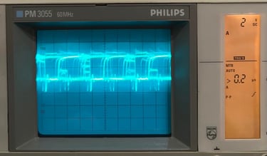
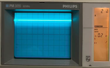
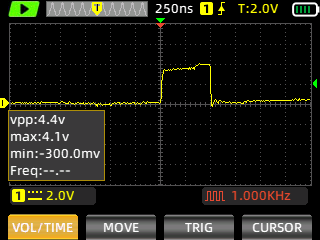
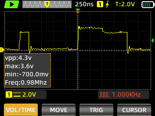
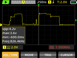
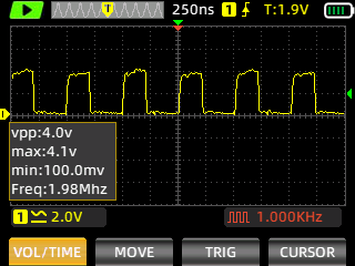
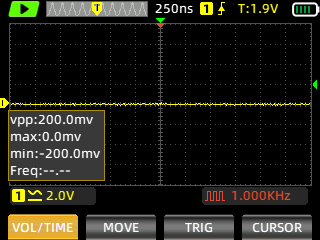
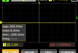
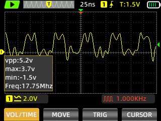
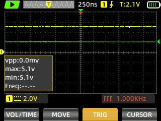
Settings on Philips/Fluke PM3055 60 MHz analog oscilloscope:
2 V / DIV
See individual pictures for time settings
Still images of the signal are captured with ZOYI ZT-703S portable oscilloscope.
Signals have been measured on a working Commodore 64 assy 250466 in idle mode (blue screen).

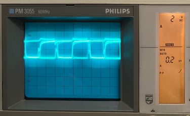
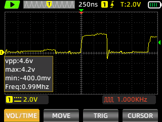
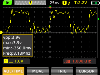
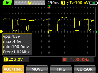
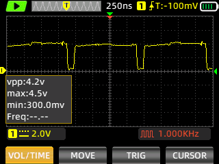
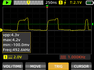
Pin #1
DB6
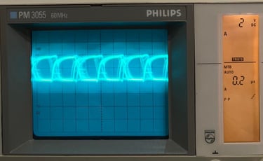
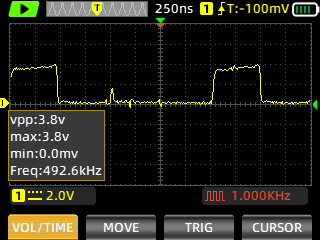
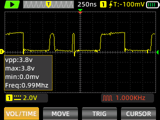
Pin #2
DB5
Data bus line #5
Direction: In/Out
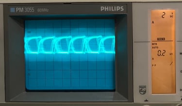
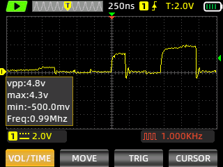
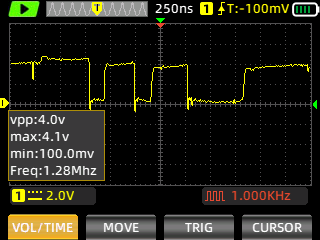
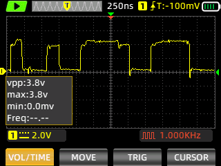
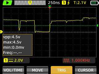
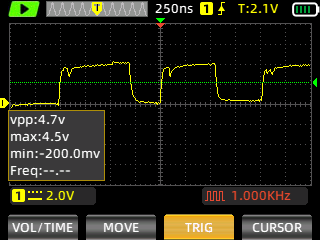
Pin #3
DB4
Data bus line #4
Direction: In/Out
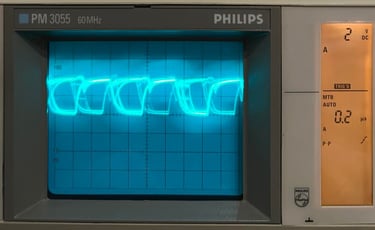
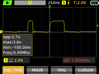
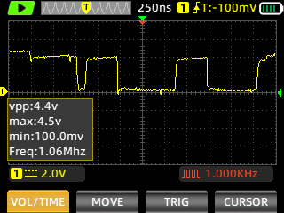
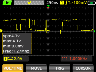
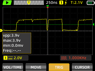
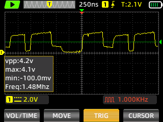
Pin #4
DB3
Data bus line #3
Direction: In/Out
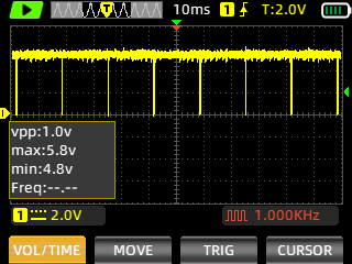
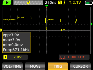
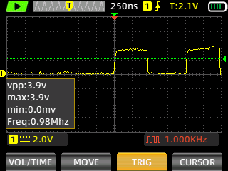
Pin #5
DB2
Data bus line #2
Direction: In/Out
Data bus line #6
Direction: In/Out
Pin #6
DB1
Data bus line #1
Direction: In/Out
Pin #7
DB0
Data bus line #0
Direction: In/Out
Pin #8
/IRQ
Interrupt ReQuest.
Direction: Out
This pin is going LOW when an interrupt was toggled in the VIC-II.
There are four possible sources for an IRQ:
rasterline, lightpen, sprite-sprite collision and sprite-background collision
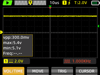
Pin #9
LP
LightPen.
Direction: In
A falling edge on this input causes an interrupt.
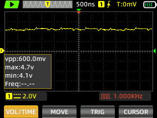
Pin #10
/CS
Chip Select.
Direction: In
HIGH=VIC-II is decoupled from bus.
Pin #11
R/W
Read/-Write. LOW=write to registers, HIGH=read from registers.
Direction: In
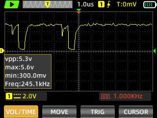
Pin #12
BA
ReaDY. When going LOW, the CPU waits after next read cycle for this line going HIGH again.
Direction: Out
If this line is low during a read access, the processor stops with the address lines reflecting the current address being fetched. It is ignored during write accesses. In the C64, RDY is used to stop the processor if the VIC needs additional bus cycles for character pointer and sprite data accesses. It is connected to the BA signal on the VIC.
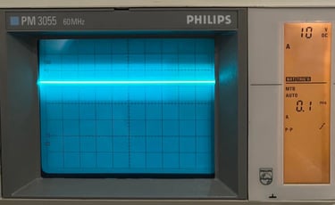
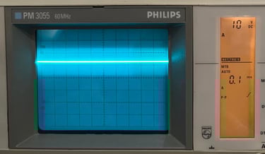
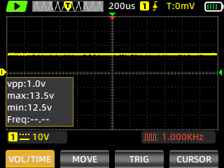
Pin #13
VDD
Reference voltage. This pin is connected to +12V DC (6567/69), or +5V DC (8562/65).
Direction: -/-
NOTE:
This is the 6569 chip in use. Therefore the VDD=12 V and the scope is set to 10 V / DIV

Pin #14
Color
Color output
Direction: Out
Pin #15
S/LUM
Sync / Lumimance output
Direction: Out
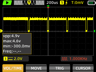
Pin #16
AEC
Address Enable Control. Directly connected with AEC of the CPU. When going LOW, the CPU puts its bus lines into high impedance state and is thus totally decoupled from the rest of the system, so that the VIC-II can take control over it.
Direction: Out
Pin #17
PH0
Phi 0. The VIC-II outputs the system clock for the 6510.
Direction: Out
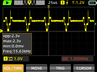
Pin #18
/RAS
Row Address Strobe
Direction: Out

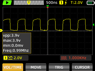
Pin #19
CAS
Col Address Strobe
Direction: Out
Pin #20
VSS
Ground (0V)
Direction: -/-
Pin #21
PHCL
Phi color. The color clock for the VIC-II. 14.31818 MHz for NTSC, 17.734472 MHz for PAL.
Direction: In
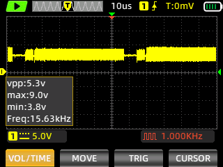
Pin #22
PHIN
Phi in. DOT CLOCK for the VIC-II. 8.18 MHz for NTSC, 7.88 MHz for PAL.
Direction: In
Note: The still image shows a PAL signal even if the calculated frequency seems to be in the NTSC range
Pin #23
A11
Address bus line #11. Bit 11 of video Address bus.
Direction: In/Out
Pin #24
A0 (A8)
Multiplexed address bus line A0 / A8
Direction: In/Out
Pin #25
A1 (A9)
Multiplexed address bus line A1 / A9
Direction: In/Out
Pin #26
A2 (A10)
Multiplexed address bus line A2 / A10
Direction: In/Out
Pin #27
A3 (A11)
Multiplexed address bus line A3 / A11
Direction: In/Out
Pin #28
A4 (A12)
Multiplexed address bus line A4 / A12
Direction: In/Out
Pin #29
A5 (A13)
Address bus line A6
Direction: In/Out
Pin #30
A6
Multiplexed address bus line A5 / A13
Direction: In/Out
Pin #31
A7
Address bus line A7
Direction: In/Out
Pin #32
A8
Address bus line A9
Direction: In/Out
Pin #33
A9
Address bus line A8
Direction: In/Out

Pin #34
A10
Address bus line A10
Direction: In/Out
Pin #35
DB11
Data bus line #11
Direction: In/Out
Pin #36
DB10
Data bus line #10
Direction: In/Out
Pin #37
DB9
Data bus line #9
Direction: In/Out
Pin #38
DB8
Data bus line #8
Direction: In/Out
Pin #39
DB7
Data bus line #7
Direction: In/Out
Pin #40
VCC
Supply voltage (+5V DC)
Direction: -/-


Banner picture credits: Xato