
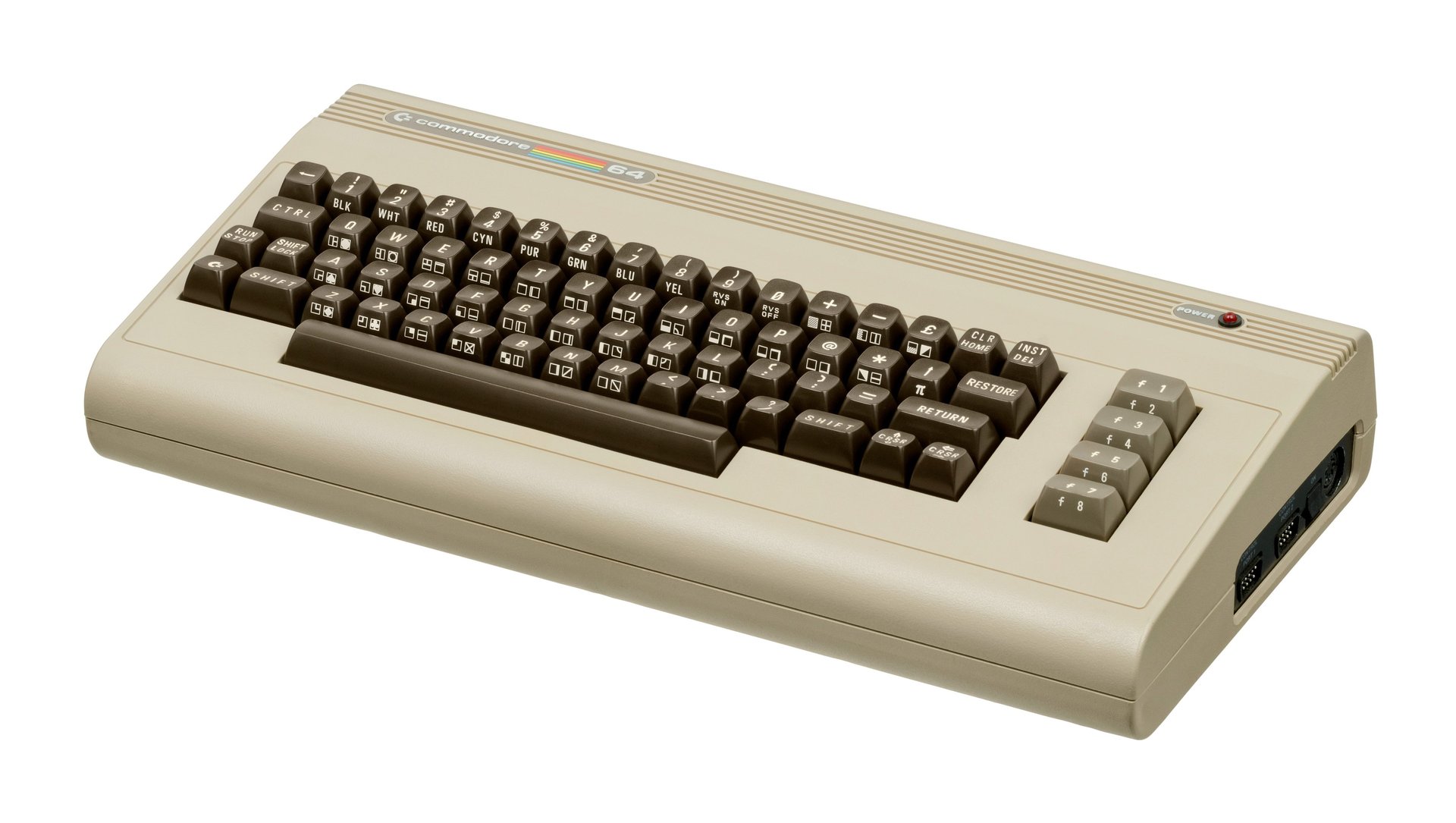
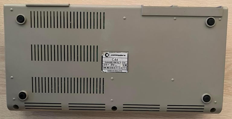
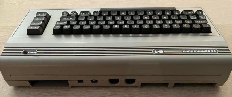
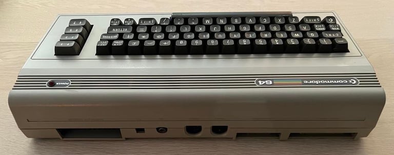
C64 Breadbin
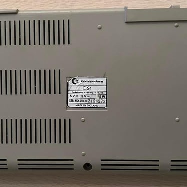
Ser. No. 2154273 Assy 250425
Refurbishment plan
To refurbish this C64 breadbin the plan is to do this trough the following steps (some of them in parallell):
- Clean and remove stains from the chassis
- Clean and restore the keyboard
- Refurbish main board (cleaning, checking, repairing, replacing capacitors and voltage regulators etc.)
- Recap RF-modulator
- Verify operation by testing
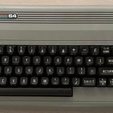
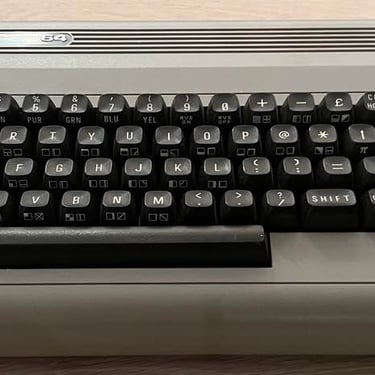
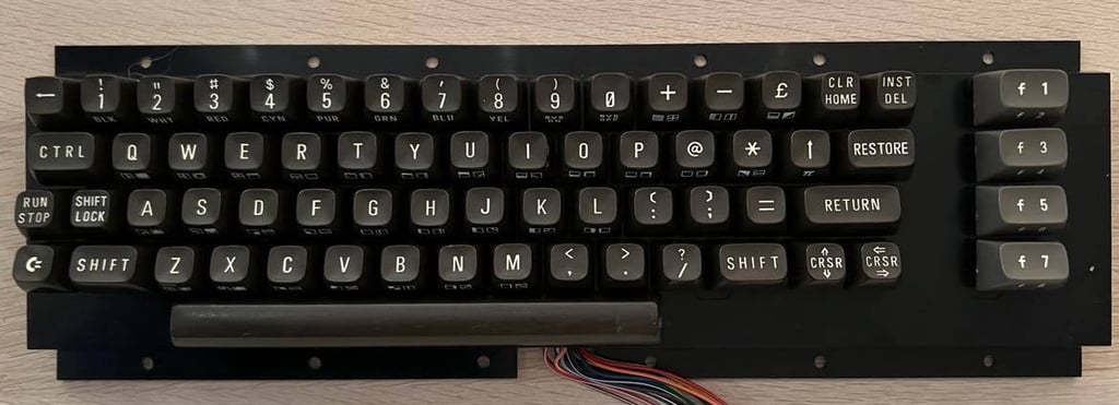
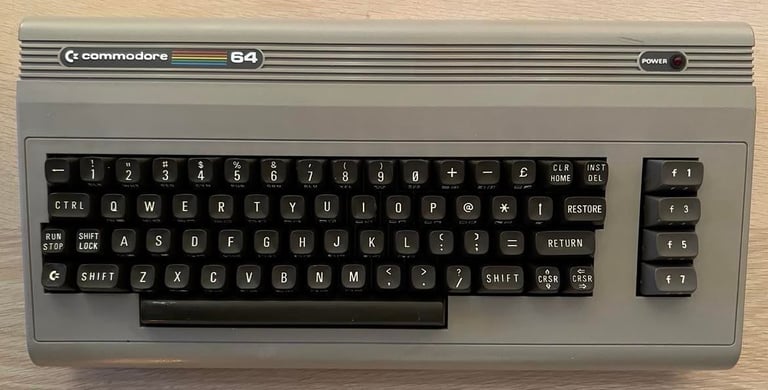
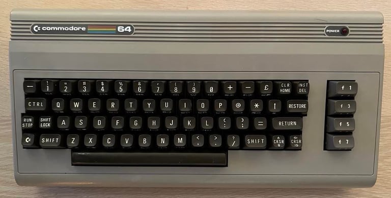
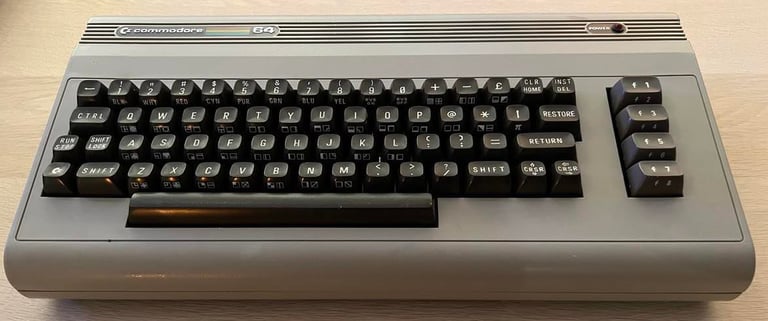
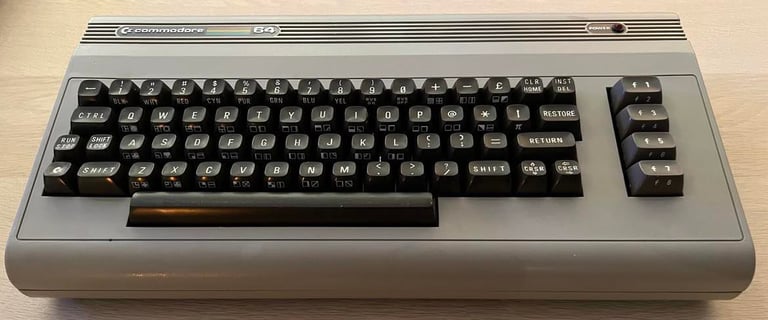
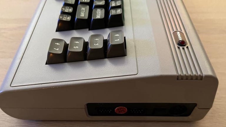
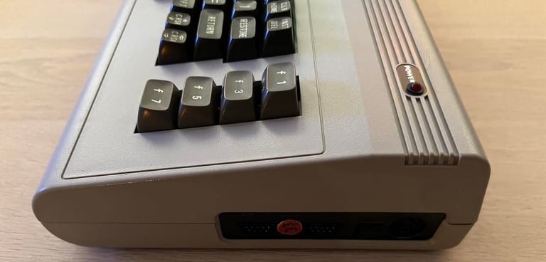
Below you will find some pictures before I begin the refurbishment (click to enlarge). This looks very promising! It´s not very dirty and looks intact.
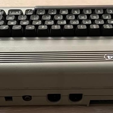
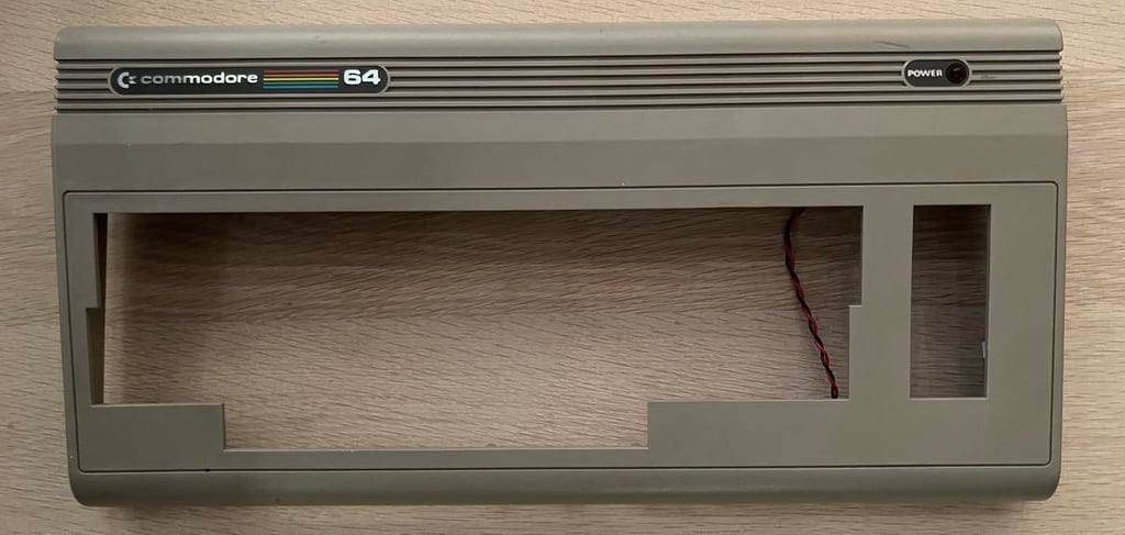
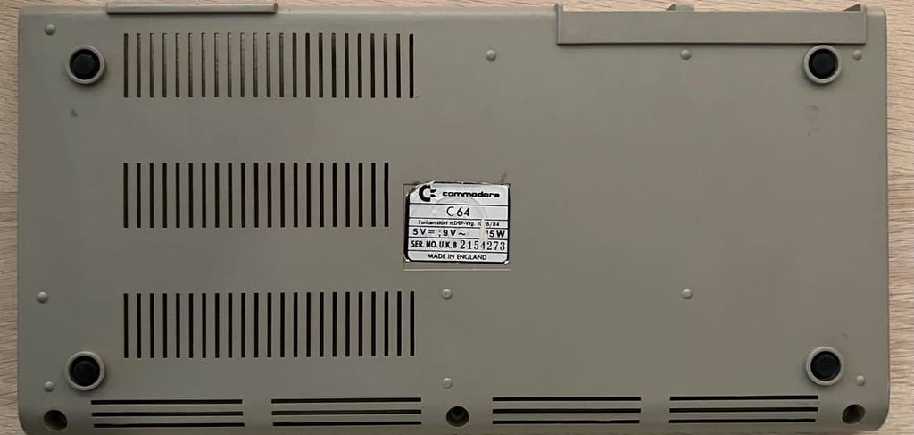
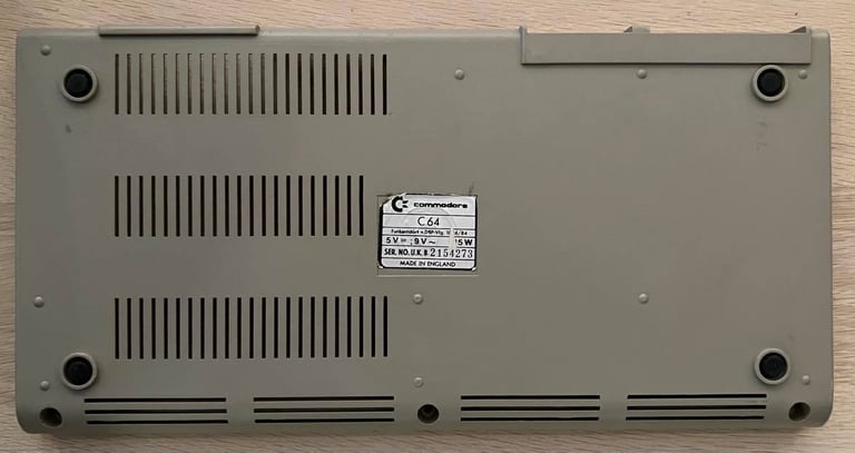
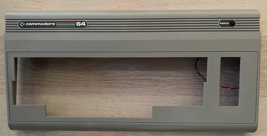
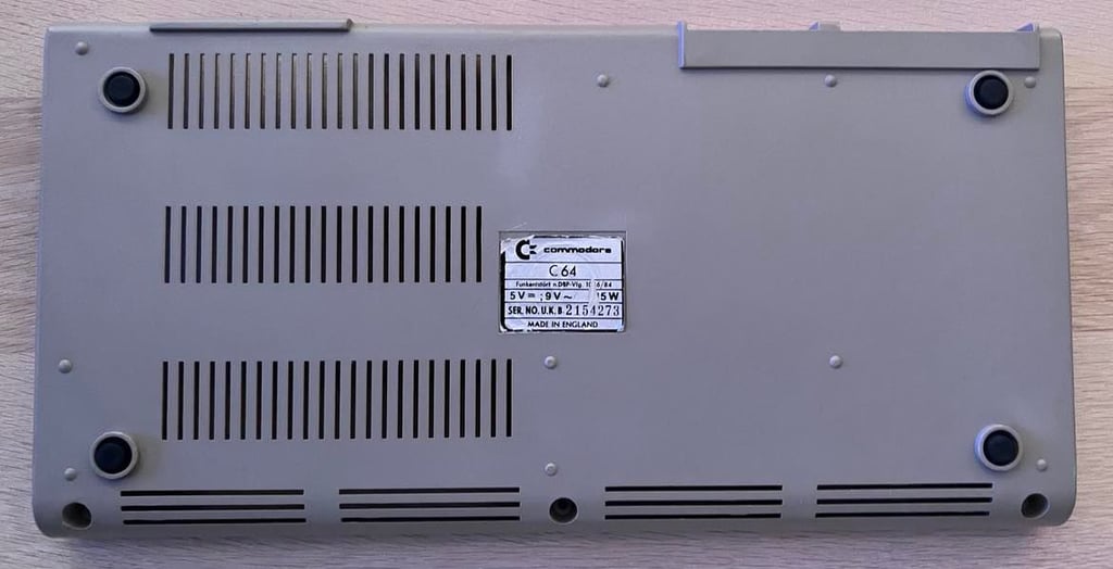
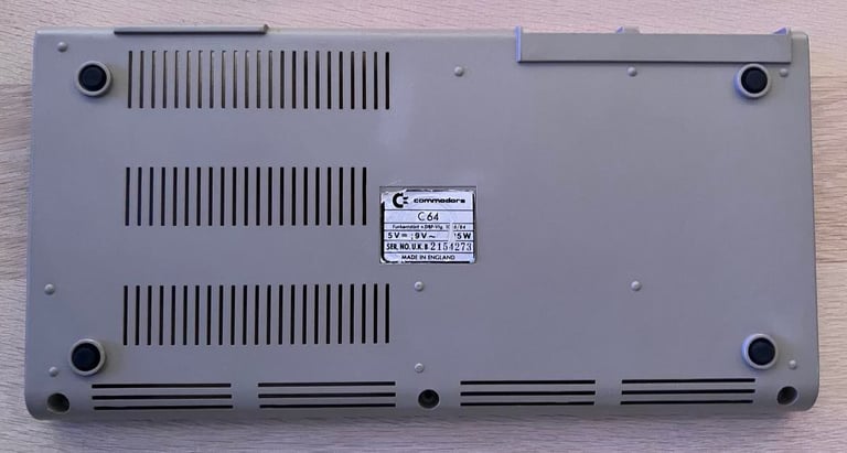
Exterior casing
The exterior casing consists of a top- and a bottom cover. To separate the casing in these two parts the three screws at the bottom are removed. Below are pictures of the casing before cleaning.

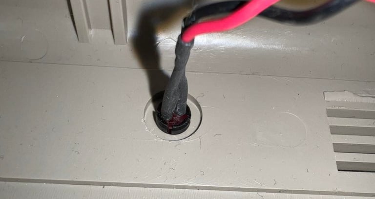
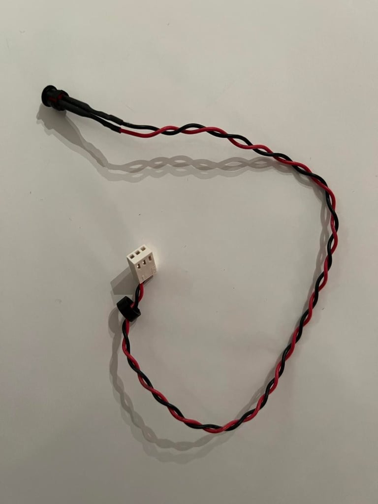
First thing to do is to remove the LED. On the backside of the top cover there is a small ring clip which is gently lifted so that it reveals another plastic clip holding the LED. When the ring is removed (more precisely: moved to the wire) the LED is pushed firmly from the topside. The LED will then pop put, and the remaining plastic clip can be removed by carefully pushing from underneath. The three pictures show (from left to right); before ring clip is removed, ring clip removed and LED cable.

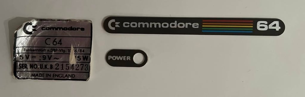
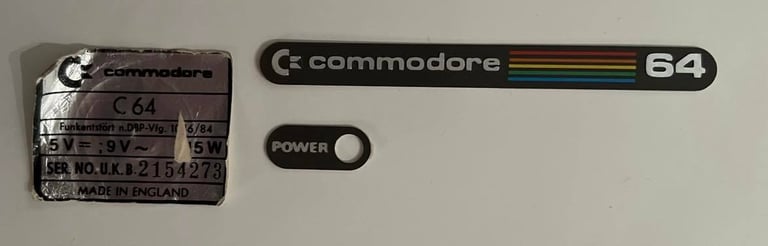
Next operation is to removed the stickers. It is not strictly required to remove the top cover stickers just for cleaning, but I have not yet decided whether to retrobright the casing or not. The stickers are carefully removed by using some heat from a hair dryer and a sharp knife. The rubber feets are also removed - but they were not present when the picture was taken:-)
The casing is cleaned with mild soap water and glass cleaning spray. Also, stains are removed with a combination of baking soda and isopropanol. Still, there are some marks on the casing which can not be removed. Well, it can be removed by sanding, but I choose not to do this. I think that the marks are so marginal that it is better just to leave it as it is.

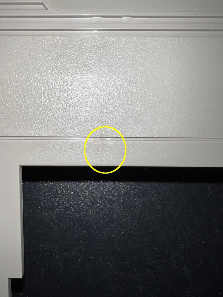
During the cleaning process I notice that there is a very small crack in the top cover. It is not very visual and big, but it is there. See picture below. I place some glue from the backside to try to prevent further cracking.

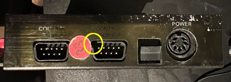
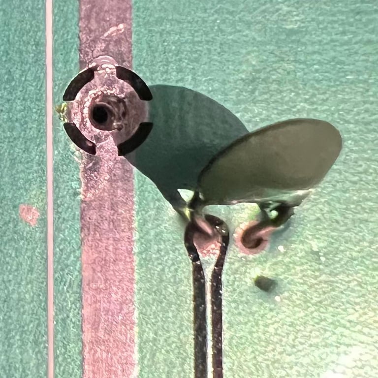
Also, there is a small piece of the plastic missing from one of the control ports. But I really don´t see this is a problem. The joystick port will function as it should without this little piece.

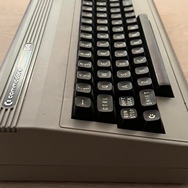
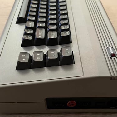
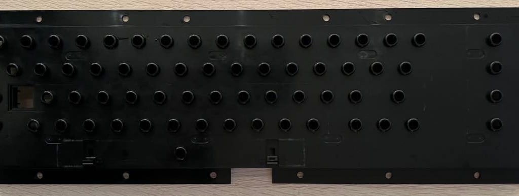
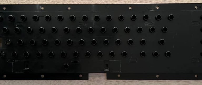
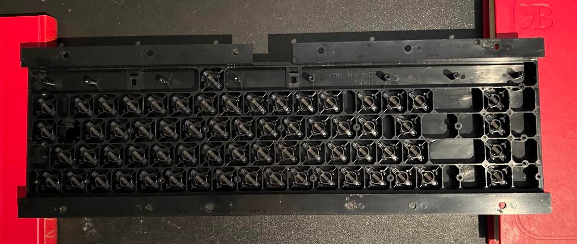
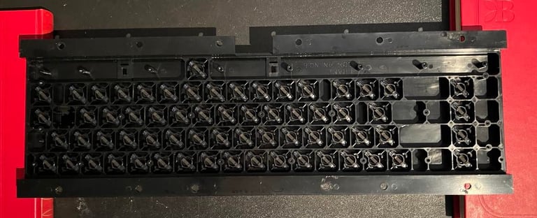
Keyboard
There are eight screws holding the keyboard attached to the top cover. These screws are removed and keyboard is loose:

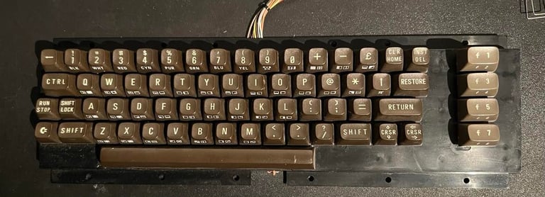
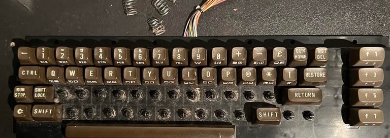
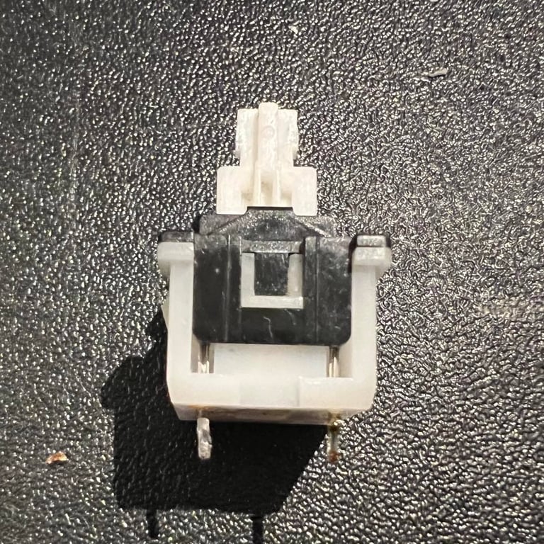
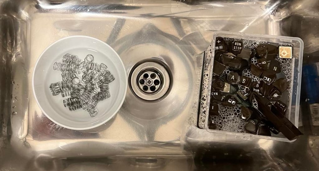
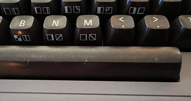
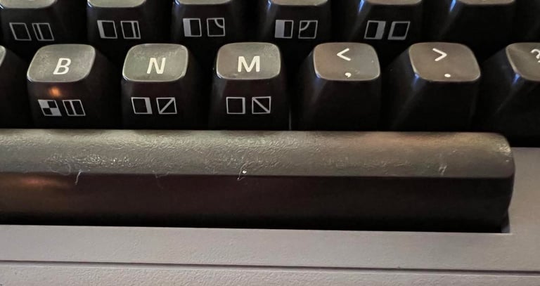
This keyboard is not bad all all I think. Yes, it´s dirty but it looks intact and no visual damage. To remove the keys I use a little tool; the keycap puller. With this tool it´s quite easy to get the keycaps off the plungers without damaging either the key, the spring or the plunger. Note that the spring for the spacebar is different from the remaining 65 keys. So it´s a good idea to place this spring in a separate plastic bag when doing the refurbishment.
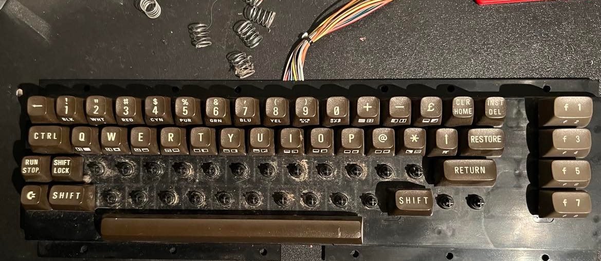
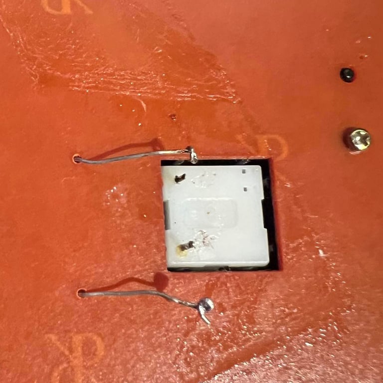
To remove the SHIFT LOCK key the two wires on the backside of the keyboard is desoldered. Then the key is pushed forward (from the backside of the keyboard). With a gentle, but firm, push the key snaps out.
The plastic bracket holding all the keys is washed with luke warm soap water. Below are some "before" and "after" pictures.
All keys are placed in a box with mild soap water for a few hours, and the springs are placed in a bowl with vinegar. The springs are not corroded as far as I can see but I do it anyhow to make sure any rust is removed. Note since vinegar is a weak acid it´s important that the springs are carefully washed with water and dried afterwards.

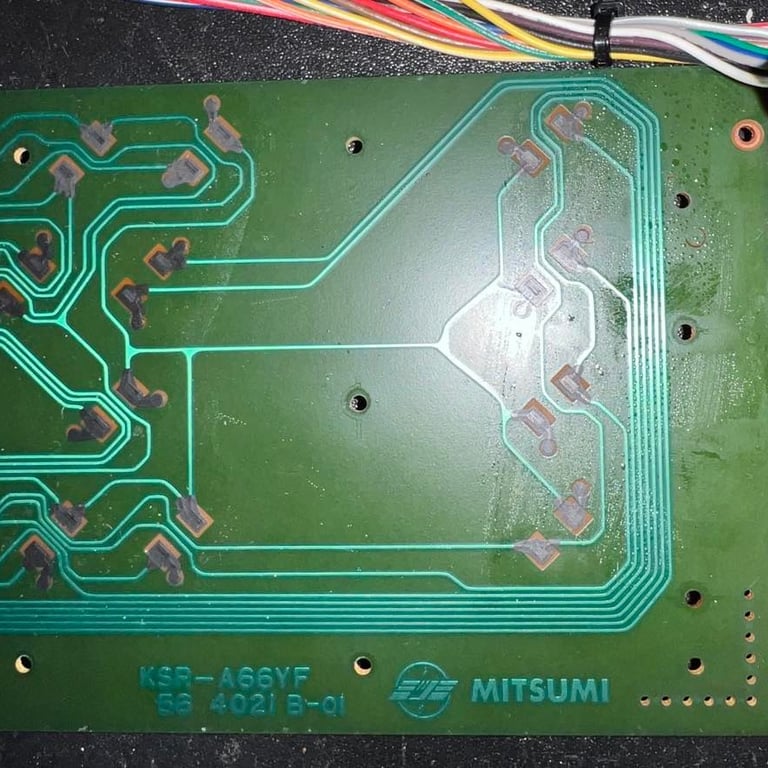
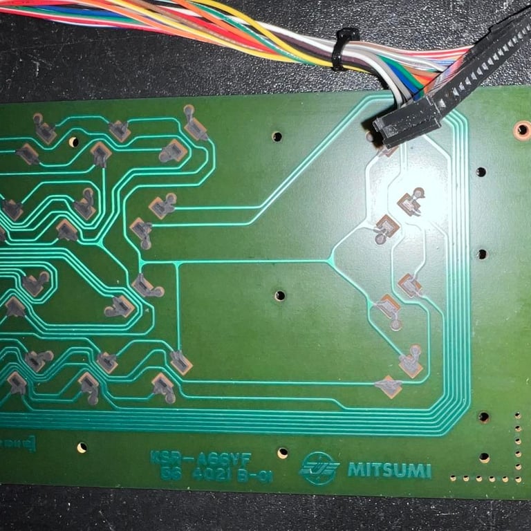
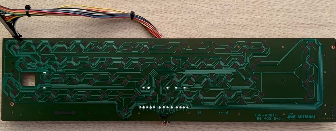
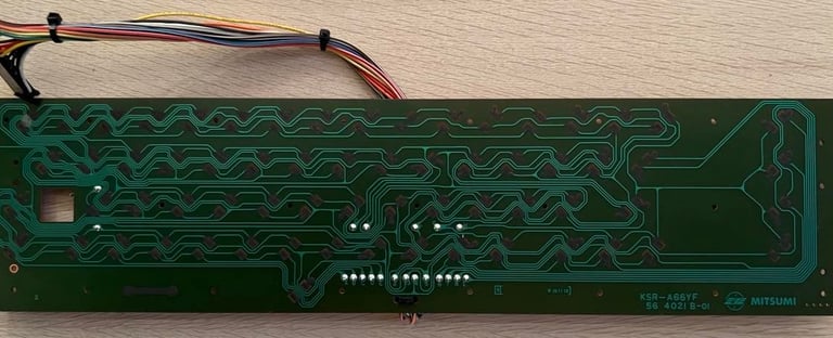
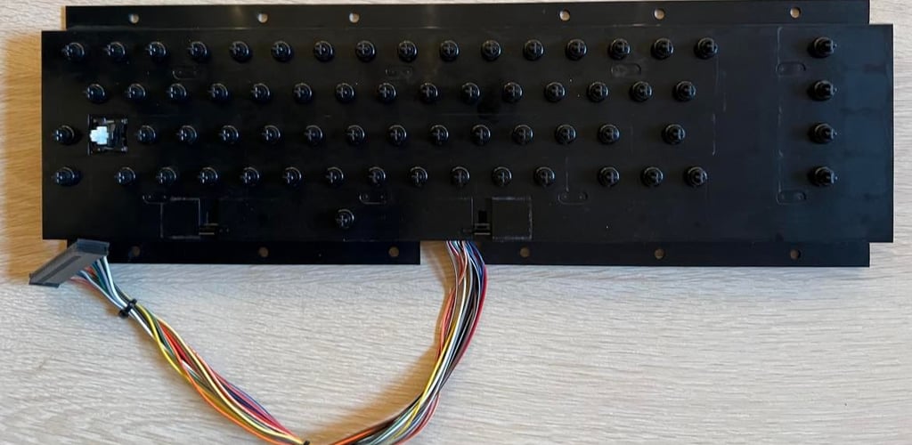
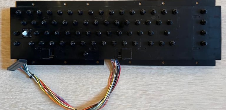
There is a PCB which creates the contacts between the plungers and the rest of the C64 (CIA#1). It looks like something have been spilled over the keyboard a some point in time, and this has come trough to the PCB. Luckily this doesn´t seem to have done any damage - no sign of corrosion. So after a good clean with isopropanol the PCB is back to it´s original state.
Below are two pictures; the one to the left shows the PCB before cleaning where the residue of the spilled "stuff" is visible, and the one to the right where the same area is cleaned. At the bottom is a picture of the complete PCB after cleaning.
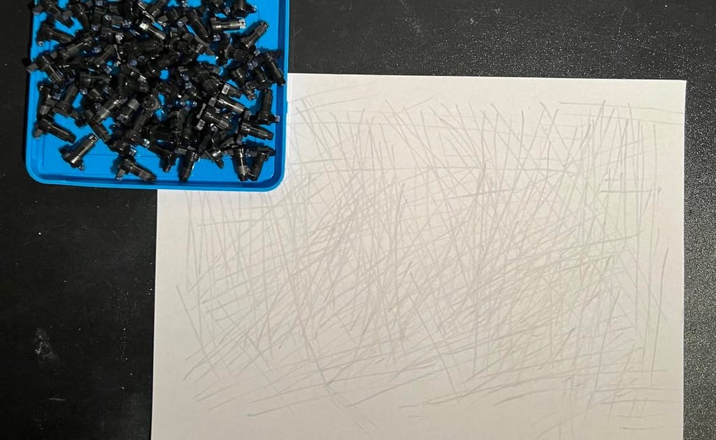
Everyone who grew up with the Commodore 64 back in the 80´s remember the frustration when e.g. space bar, return or other keys had to b pressed really hard to work. I use a method to revive the plungers which brings the plungers back to life. That said, there are different ways of doing this - and probably different meanings on what is the best / worse method. But the way I do this is by gently dragging each plunger over a piece of paper to remove dust, grease and loose carbon. My experience is that this works good, also don´t damage the contact at the end of the plungers.

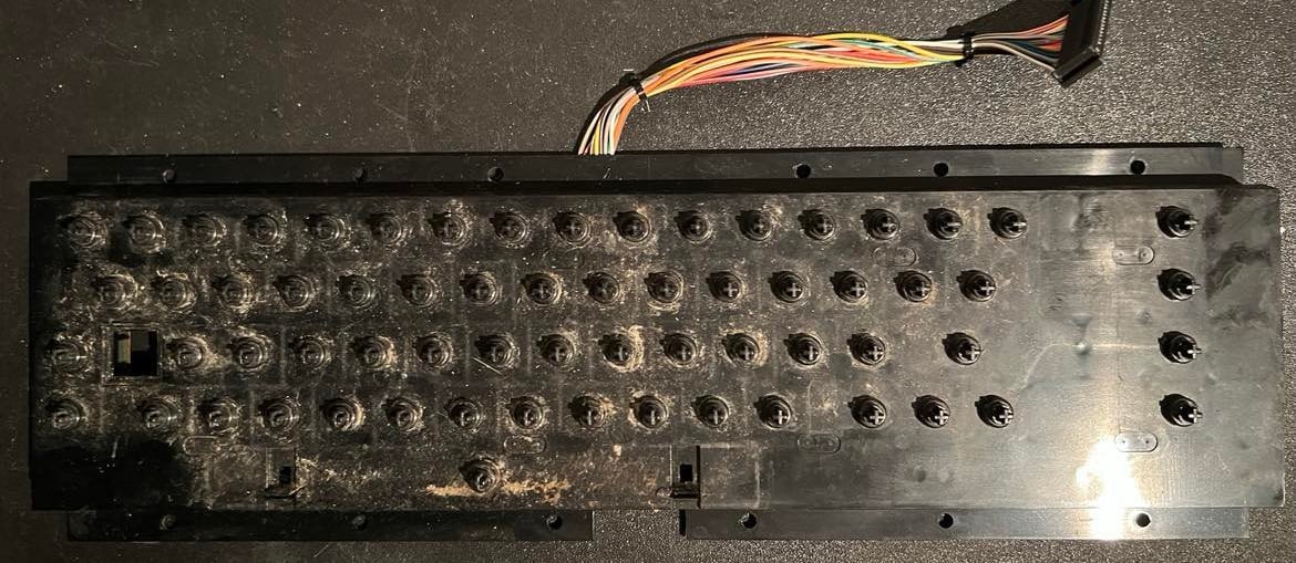
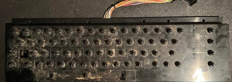
The plungers are put back in the plastic chassis/bracket after this operation, and the PCB is screwed back in.
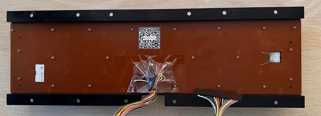
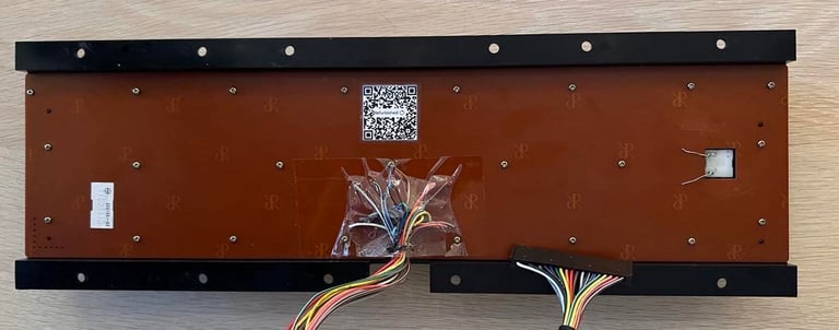
All keys are put back and a small QR code sticker is placed on the backside. The QR code links to this webpage for future reference.

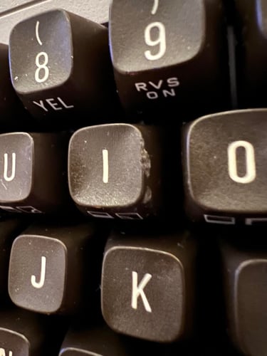
There are some marks on some of the keys which are not possible to remove. They do not affect the performance of the Commodore 64 in any way (they are purely cosmetic), but they are there. It´s most visible on the "I" key and the "Spacebar" key.
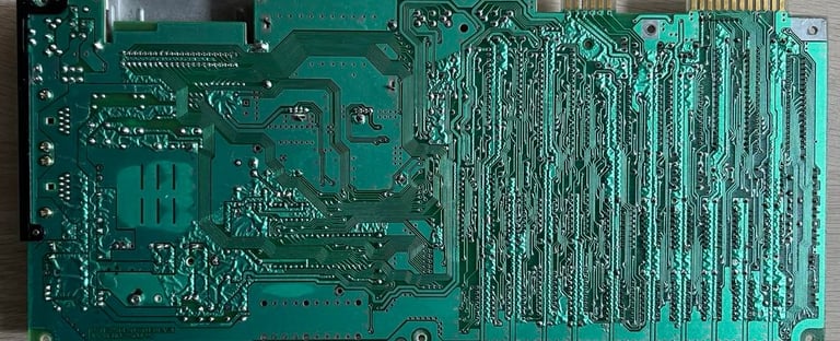
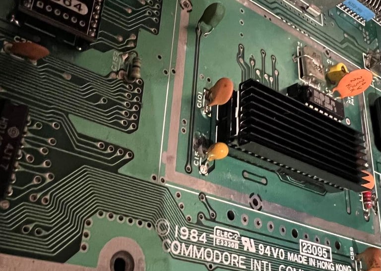
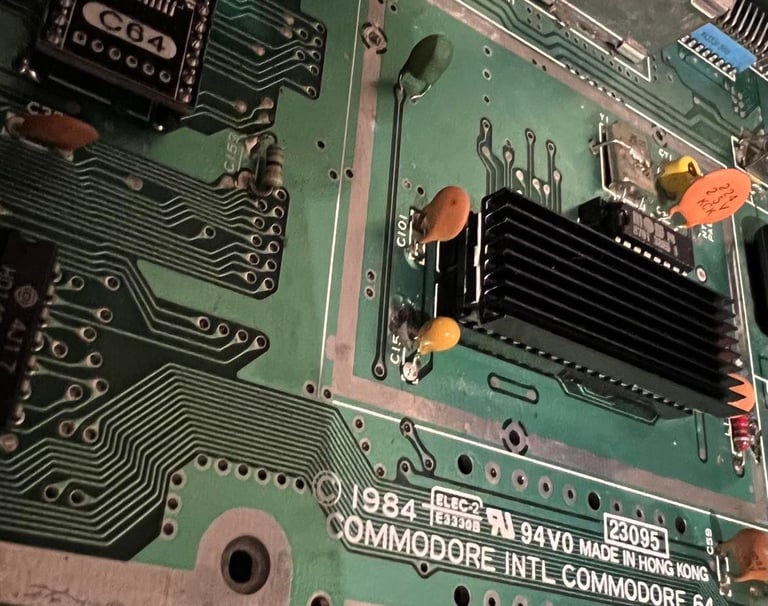
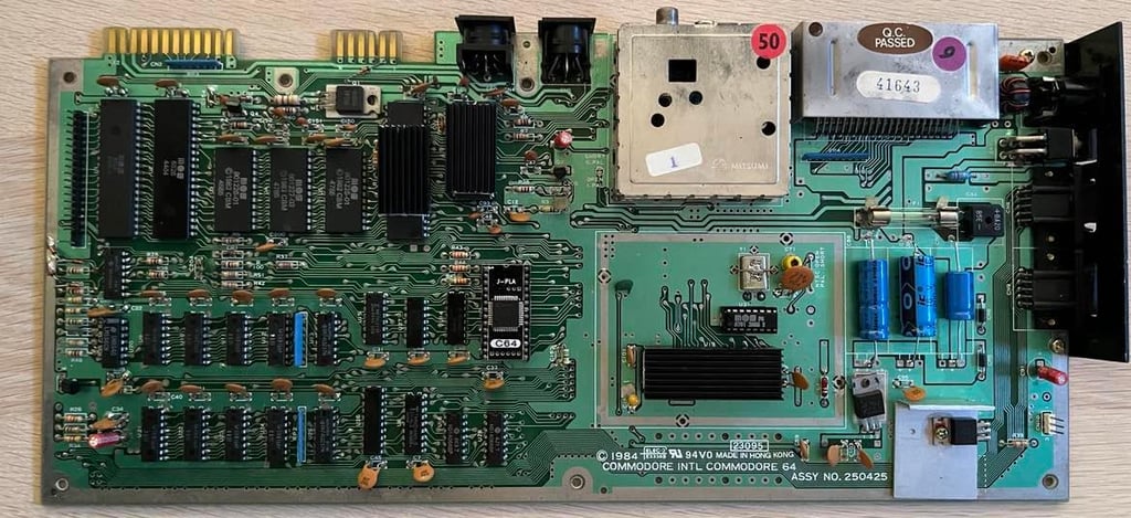
Mainboard
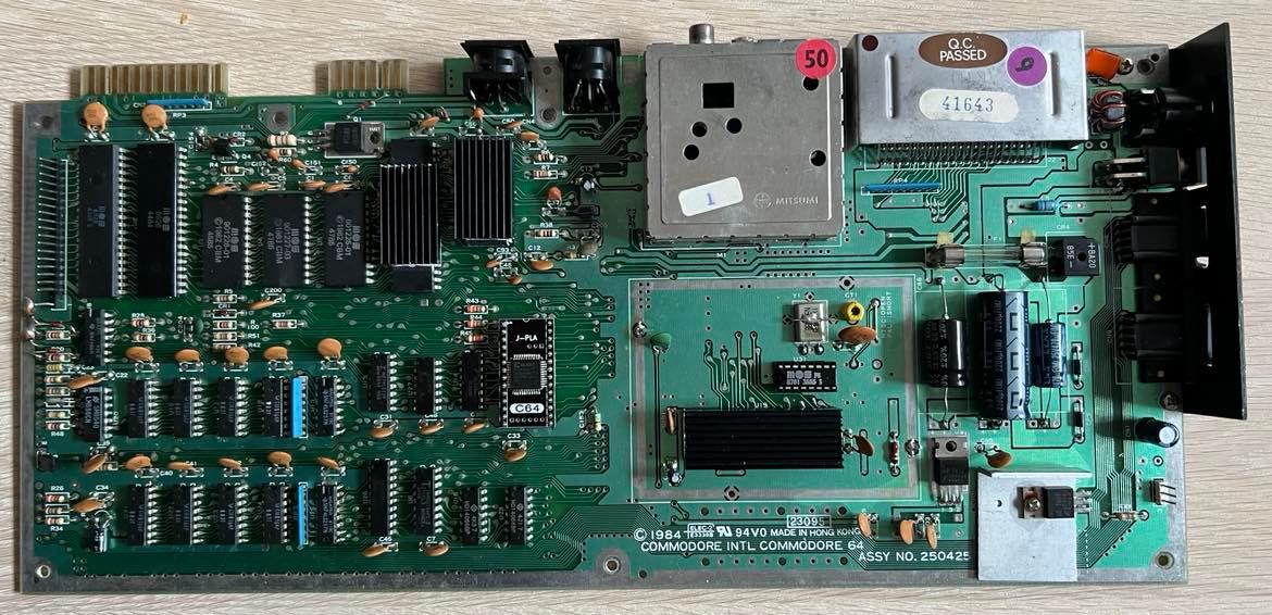
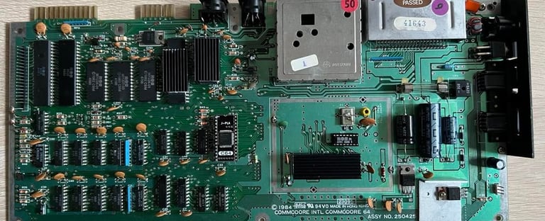
This mainboard is an assy 250525 and my guess is that it´s made sometime around late 1985. The ROM chips does not seem to be replaced since factory and are manufactured week 45-47 in 1985, and the CIA#1 chip is also from 1985.
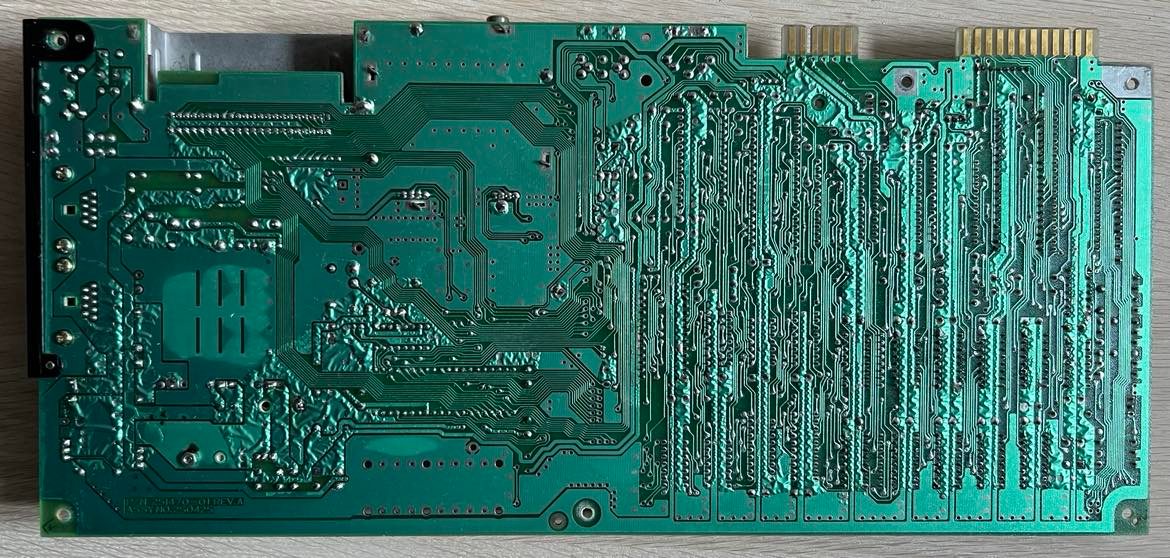
First thing is a visual inspection of the main board. I notice the following:
This mainboard have been repaired/service before
The PLA is replaced with a new modern variant: J-PLA. Unfortunately it is not socketed. Only soldered directly to the mainboard. Not a big deal, but I like to use sockets when chips are replaced.
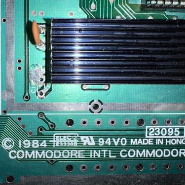
CPU-, SID- and VIC-II chip have heat sinks
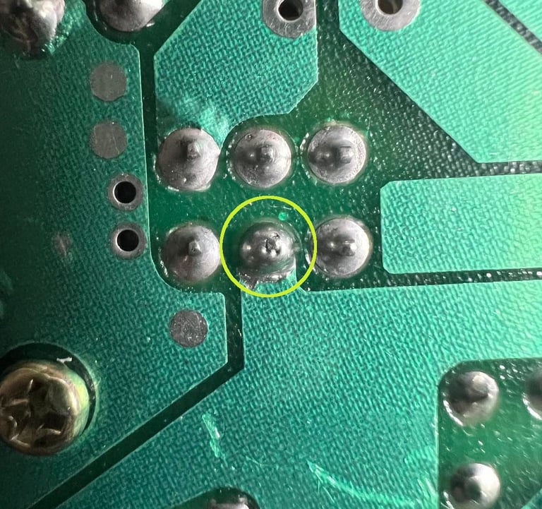
CIA#1 chip (from 1985) have probably been a faulty candidate during repair. Pin #1 (VSS +5V) has been cut and soldered back. This is a normal way of testing chips during fault finding. Nevertheless, it doesn´t seem to have been desoldered and replaced.
CIA #2 chip (from 1984) have probably been replaced (with an older chip). It is not socketed - and the soldering job is good. So this work is done by a professional or a good amateur.
Some (all?) of the electrolytic capacitors have been replaced. I´m not sure what has been done here. The brands used and the soldering work is very varying (from bad to ok - but not great). I think I will replace these anyway to make sure nothing is broken or wrong with these.
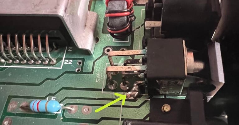
There are some odd soldering around the main switch. My guess here is that someone have soldered some of the trough holes which sometimes are left open at production time. Not a big deal probably, but I think I will clean this up.
An electrolytic capacitor has been used for C15. This is not correct. This should be a tantalum capacitor. I will replace this.
The RF-shield around the VIC-II area is removed. I like that - but I will clean up some soldering residue. The RF-shield has no meaning in 2022 - it will only accumulate heat which could damage the VIC-II.
Below are some pictures showing these visual findings (click to enlarge).
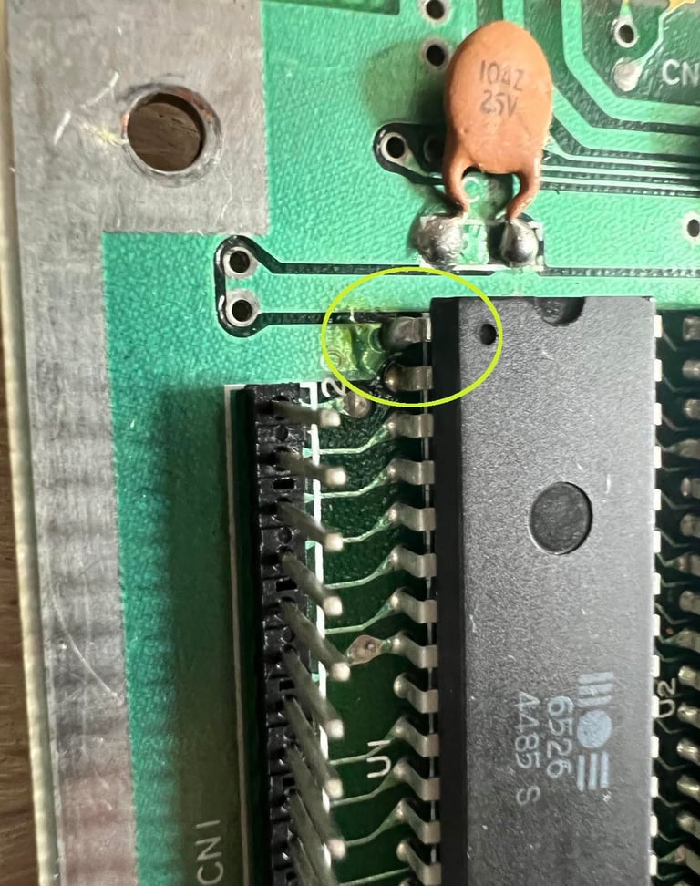
Pin #1 is cut and soldered back in (see circle). This is (was?) a normal procedure for fault finding. When pin #1 is cut the +5V is disabled making the fault finding easier.
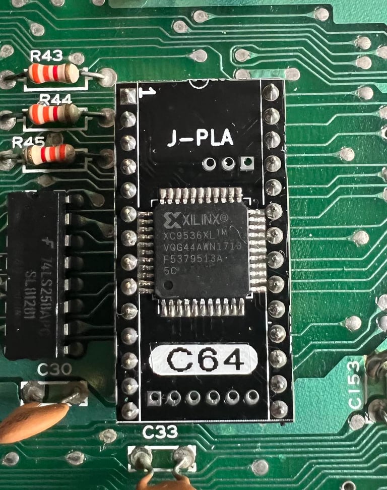
Original PLA is replaced with modern J-PLA. It is very common that original MOS PLA fail - so this replacement is very welcome.
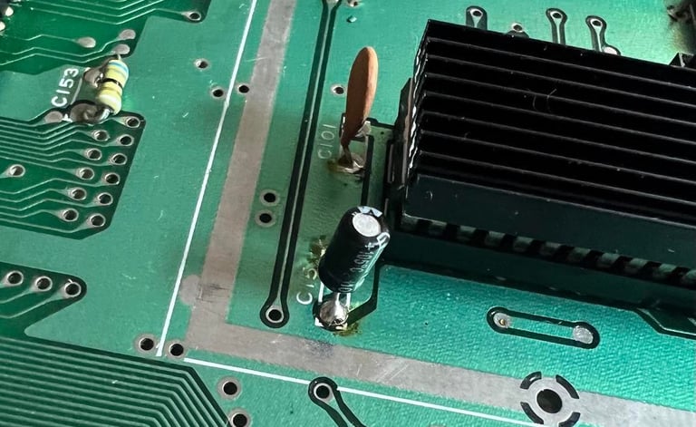
An electrolytic capacitor where a tantalum capacitor should be. This is probably not a real problem since a tantalum capacitor is in fact a polarized electrolytic capacitor, but I still think that this should be replaced with the correct capacitor.

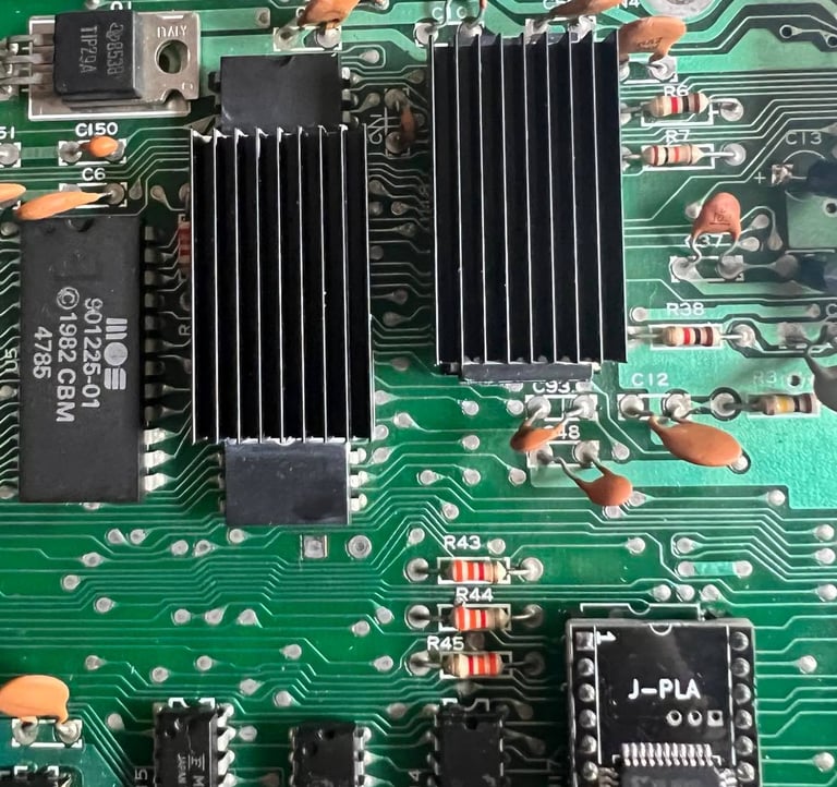
Heat sinks placed on the CPU- and SID chip.
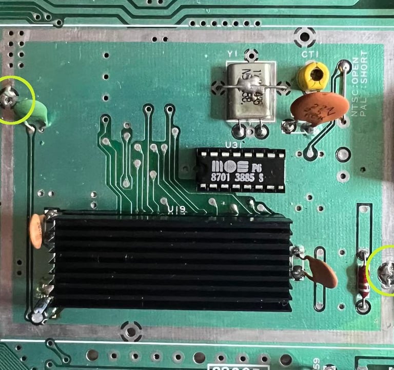
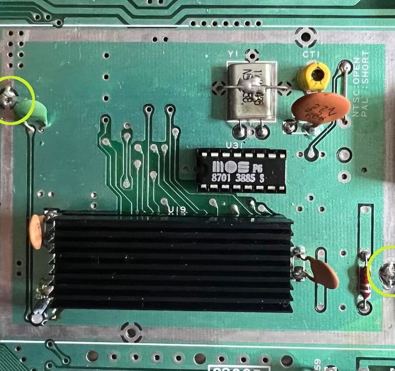
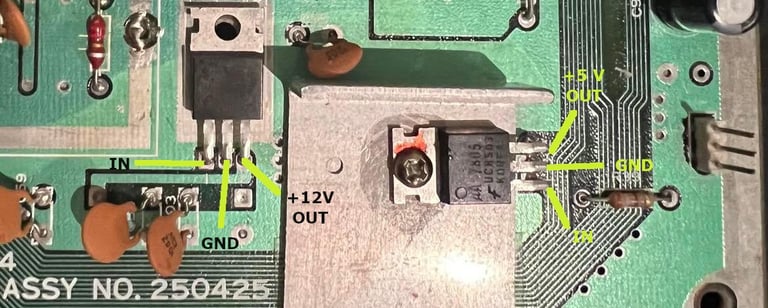
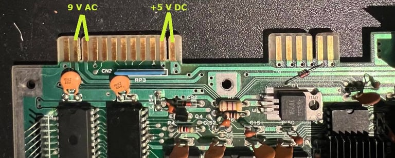
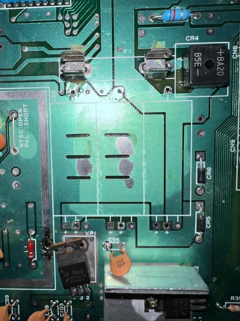
Next step is to check for short circuits, and if none, check the voltages. There are four places I check for short circuits (and check voltages):
Between ground (GND) and IN / OUT (+5V) from 7805 voltage regulator
Between ground (GND) and IN / OUT (+12V) from 7812 voltage regulator
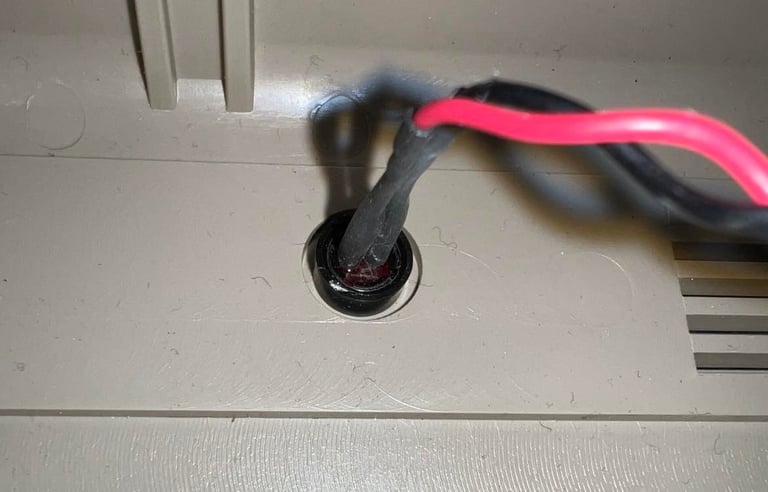
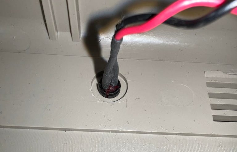
Between ground (GND) and + 5V at the User Port (from PSU)
Between the two AC (9 V) phases at the User Port (from PSU)
Pictures below shows the position of these. The first shows the voltage regulators, and the second shows the user port.
No short circuit is found. Voltage is applied from the PSU and are measured as in the table below.
RF-shield is removed which is good. This have no real usage anymore and will only work as a heat trap. I will remove some of the residual solder (see circles). Also, as the picture shows the VIC-II chip have a heat sink.

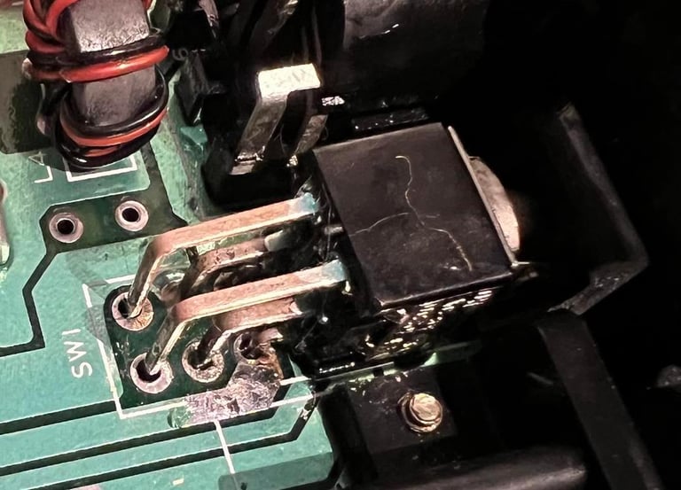
There is something dodgy around the power switch. To me it looks like some points have been resoldered, but not a very good job. The switch doesn´t look to be removed.

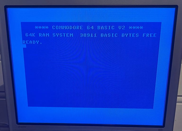
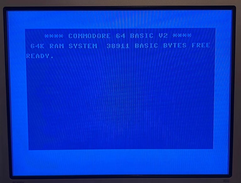
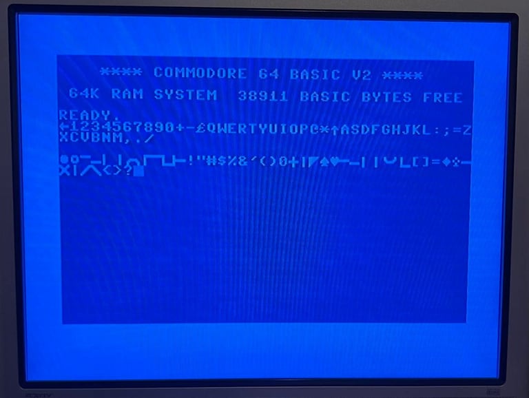
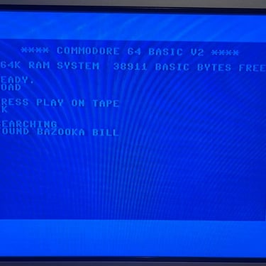
OK! It´s time for testing with a TV connected. Does it work? YES! There is a blue screen! 38911 kB BASIC bytes free! It doesn´t mean that nothing is wrong with it, but this is a very good start! There is obviously something wrong around the power switch area because if I press hard around here the C64 goes black - and needs a complete power recycle to start. But it could be due to bad soldering in this area. Anyway, below is the picture of the beloved blue screen.
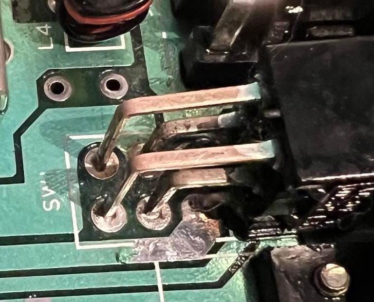
I start with the power switch problem - or more precise: the C64 goes black when pushing the PCB in the power switch area. My guess is that due to bad soldering there is either an intermittend short cut or a circuit break. The solder from the six pins are removed from the bottom side of the PCB using the desoldering gun. And the residual solder is removed from the top of the PCB. Below is a picture from the operation where most of the solder is removed.
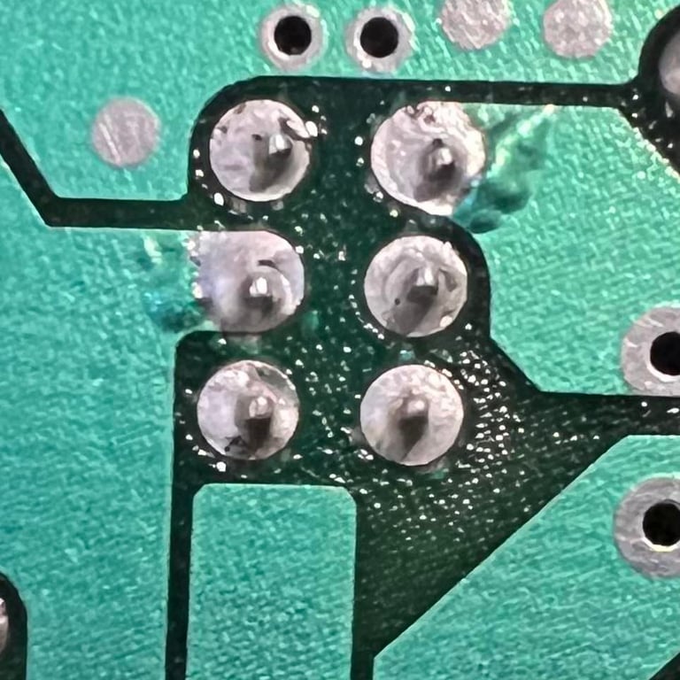
After cleaning the area (both on top and bottom of the PCB) the power switch is soldered back in. Looks way better now - not solder all over the place.
When testing the C64 after this operation I can no longer get the black screen - problem is probably fixed! Even when I push (hard) in the power switch area the C64 does not fail. But I will keep an eye on this while continuing the refurbishment.
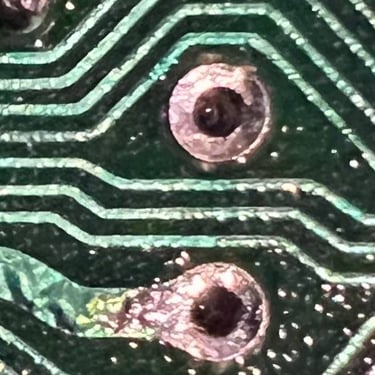
Next step is mostly for cosmetics, but I clean up the area around the VIC where the RF-shield was placed. To me this looks like a "brute force" job done previously. Half of the pad around the right side is broken in half, and a bit of the old pin from the RF-shield fall out of the left side when cleaning up and desoldering. Pictures below from this clean-up operation.
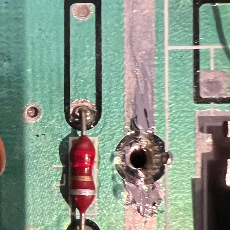
As mentioned there is an electrolytic capacitor (C15) to the left side of the VIC-II chip. This is probably not a big mistake, but the correct is to use a tantalum 4.7 uF 16 V 20% (check C64 service manual page 29). I replace this electrolytic capacitor with a tantalum - but with a slightly higher voltage: 25 V. Note that a tantalum capacitor is also polarized so the "+" and "-" needs to be in the right place.
There are quite a lot on solder on both the top and bottom of the PCB where the electrolytic capacitor is. When I desolder this capacitor some of the marking saying "C15" disappear after cleaning, but it is only cosmetic. Other than that the desoldering and soldering of this new tantalum capacitor is ok. See pictures below.
I start the process of replacing all the electrolytic capacitors. Even though I think that some of them have been replaced previously I choose to replace them all. There are quite some poor soldering - and I even notice that "wrong" capacitors have been used. Not wrong in regards of capacitance, but in voltages. E.g. the 2200uF capacitor should be rated to 16V, but it is 50V which is used. It´s not a big problem, and using slightly higher voltages are ok, but I think this is wrong. If you check Breadbox64 you can also see from the pictures there that it should be a 2200uF 16V.
Also I notice that under the large capacitors (2200uF, 1000uF and 470uF) there are signs of previous leakage. Unfortunately I forget to take a picture before cleaning, but below are two pictures; one after cleanup and one with new large quality capacitors (Panasonic Vishay) in place.
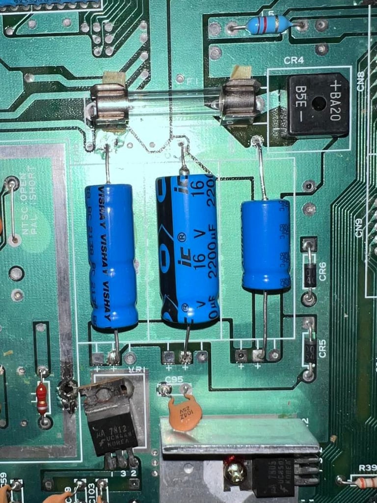
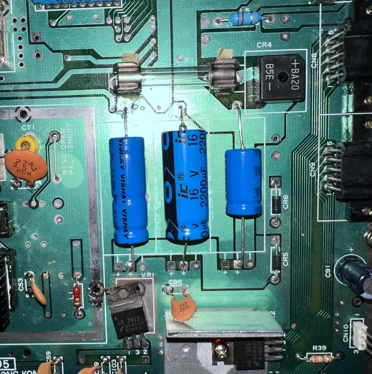
The rest of the electrolytic capacitors are replaced also with quality caps. There are only six in total on this assy - check the reference page for details. Nevertheless, it is not so easy to desolder these. It varies between the different boards and some boards require more patience (and some more heat) to remove and replace the capacitors. Below is a picture of the PCB with the new electrolytic capacitors installed.

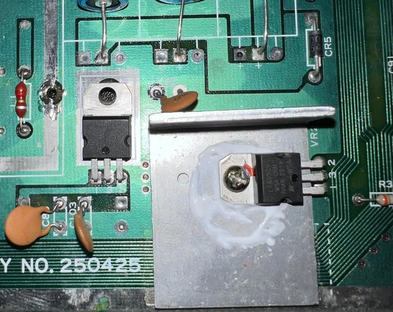
There are two voltage regulators on the mainboard. A 7805 (5 V) and a 7812 (12 V). These two are used to supply voltages to the VIC-II and SIP chip. These are (probably) old and should be replaced, and new heat sink paste should be applied since this has dried out. Notice that it is only the 7805 regulator which is attached to a heat sink. The 7812 regulator is "floating" free on the mainboard. This is correct - it is how it is done at time of manufacture. Below is a picture of the new voltage regulators in place.
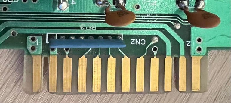
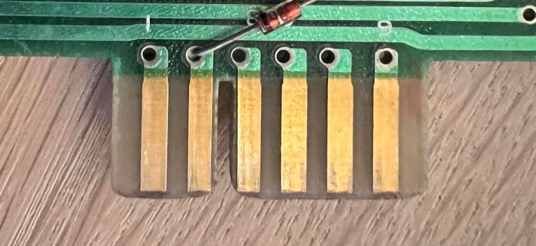
Both the user port and the datasette port are cleaned properly. It is crucial for these to be cleaned in order to provide good connectivity to Commodore peripherals. To clean these port I first rub them (carfeully) with a rubber eraser. Then they are cleaned with isopropanol and a Q-tip.

UPDATE: The VIC-II chip in this machine is switched the VIC-II in C64 Ser. No. 606581. Why? Well, the VIC-II in this C64 have some artefacts when scrolling graphics. I´m not really sure, but my guess is that is has something to due with the surround components (capacitors, resistors, crystal etc.) which are slighty "off" - and a result creates glitches.
But does this mean that the same problem is transferred to this? No. There are no visual degrading of the graphics at all as far as I can see. The VIC-II works as it should in this machine. Below is a picture of the "new" VIC-II chip installed.

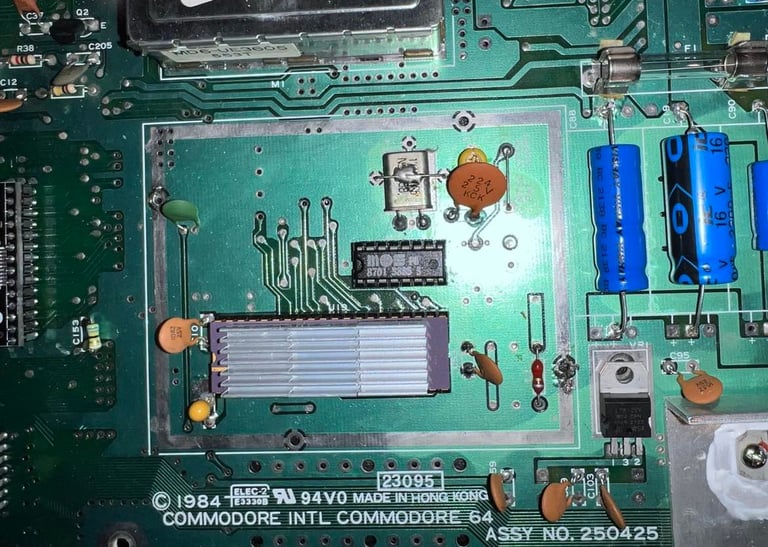
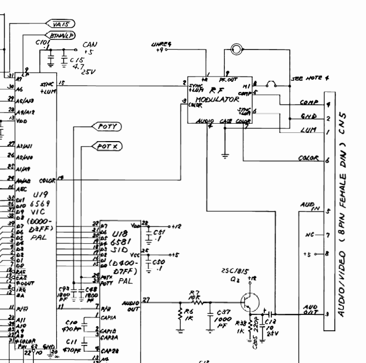
RF-modulator
The RF-modulator is responsible for creating the combined audio-and video signal from the VIC-II and SID chip. And to expose this signal trough the A/V port and RF-out. And since these are analog signals I highly recommend to also change the electrolytic capacitors in the RF-modulator. In the schematics below (borrowed from the Service manual C64/C64C) you can see how the RF-modulator combines the analog signals from the VIC-II and SID chip.
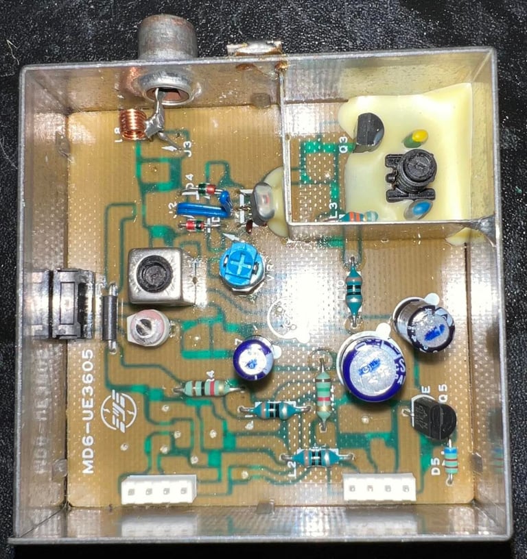
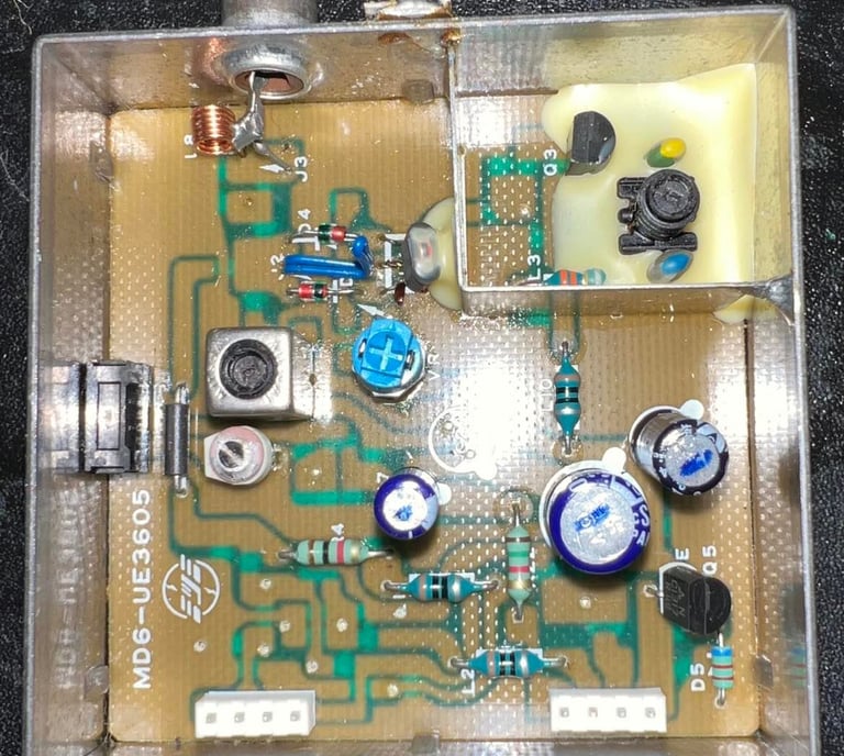
This RF-modulator is version MD6-UE3605 from Mitsumi - list of capacitors here.

Desoldering the RF-modulator is not trivial. There is a separate PCB within the RF-modulator casing which is "floating" inside, and is connected to the mainboard trough eight small pins. Also, there are four large pins from the RF-modulator casing which is soldered to the main board. These large pins requires quite some heat to free from solder. And last there are four tabs (not soldered) which are bent in position to lock the RF-modulator in place.
Nevertheless, it is of course possible to desolder the RF-modulator but the key word is : patience. If you rush this you will most likely destroy something - either pads, traces or the interior RF-modulator PCB.
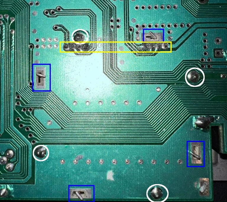
Below is a picture of the backside of the mainboard PCB where the positions of tabs and pins are located:
Blue squares: four tabs that needs to be aligned with the hole using a needle plier.
White circles: four large pins which needs to be desoldered. I use a desoldering gun - while at the same time holding a soldering iron tip on the point - to clear the pin.
Yellow square: eight small pins which connects the internal RF-modulator PCB to the mainboard PCB. I use only the desoldering gun (with about 390 degrees) to clear the pins.
Now, to remove the RF-modulator casing I carefully pry a small flat screwdriver between the casing and the mainboard. And while I do that I apply hot air around the pins in near proximity. This is a quite time consuming process and patience is required. I need to carefully to this on all edges in a circular way - and after some time the casing starts to loosen.
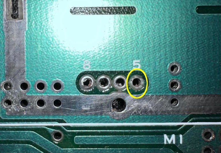
Even if I do this with great care I see that I manage to break a pad on the top of the mainboard side. This happens from time to time. But, this pad is not "used" for anything so I don´t need to use a bodge wire. The pad which is used to transmitting the signal between the mainboard and RF-modulator is on the bottom side of the PCB. Below is a picture of the missing pad and the RF-modulator removed.

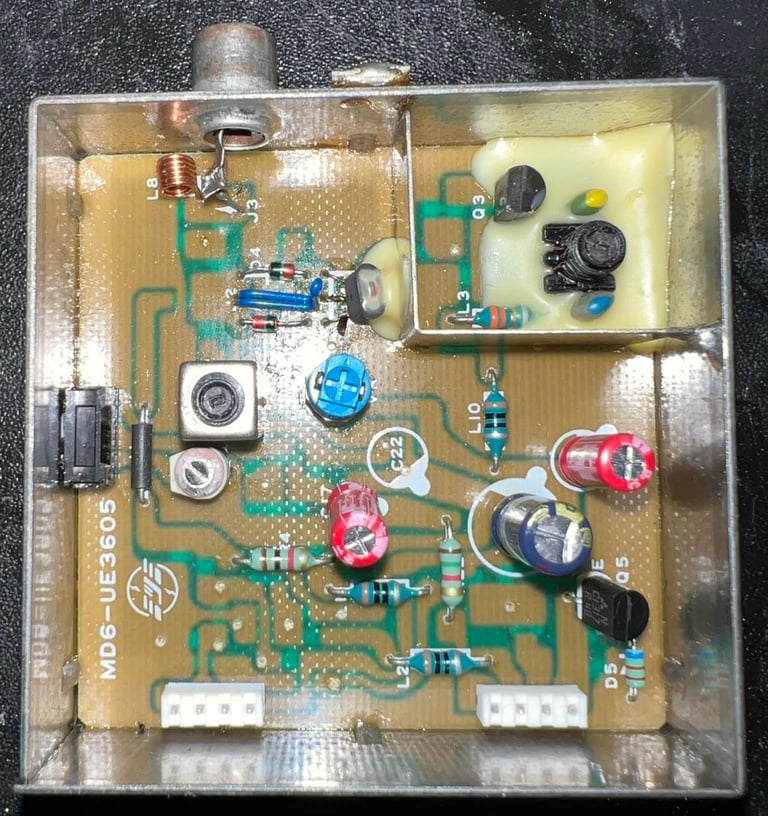
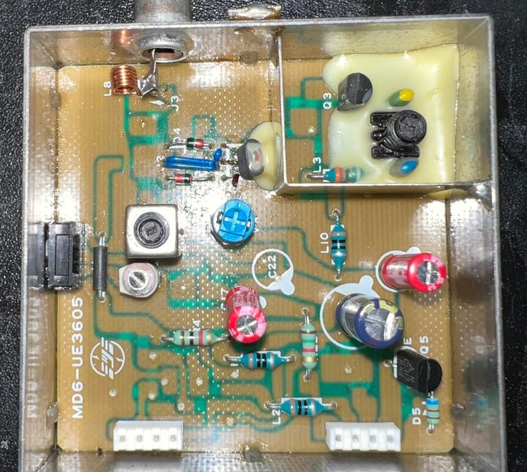
The three capacitors are replaced with new quality caps. And then the RF-modulator is soldered back in to the mainboard. Picture to the left shows the RF-modulator with old capacitors, and the picture to the right shows the modulator with new capacitors.
NOTE: after the RF-modulator is re-installed all voltages are measured again - and the voltage table in the previous chapter is updated.
Testing
Testing is done through two main stages:
Testing the basic functionality and chips
Testing by using the machine playing demos, games etc. to verify correct operation
Basic functionality and chips
The first test is done by using the Dead Test Cartridge. This test will check the basic functionality of chips such as VIC-II, CPU, SID, CIA#1/2 and RAM (inc. COLOR). Nevertheless, it will not test everything that these chips can do. The dead test pass without any faults detected.

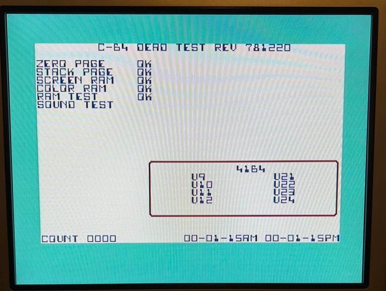
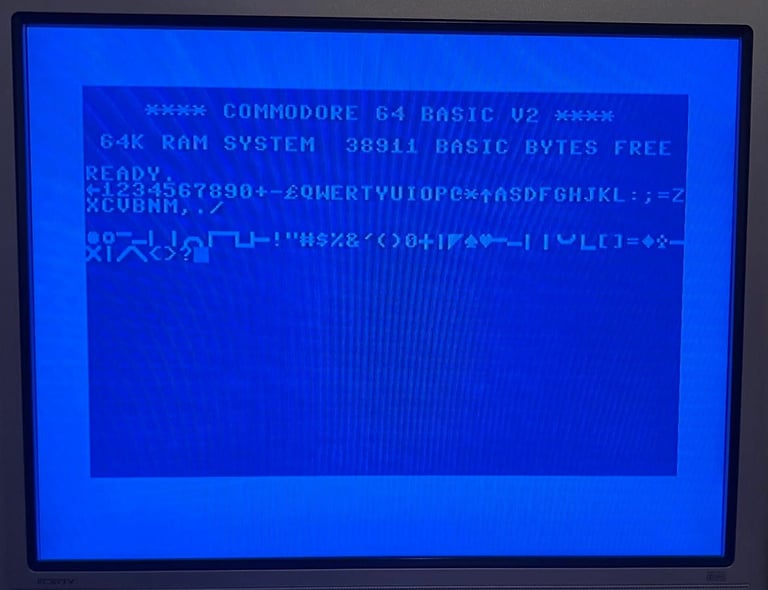
Next test it to check that normal startup screen is ok (with 38911 kB RAM Free and blinking cursor). Also, the keyboard is checked. All pass without faults.
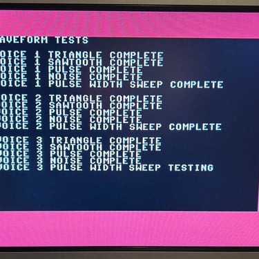
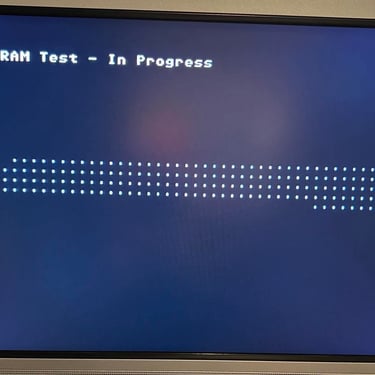
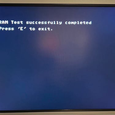
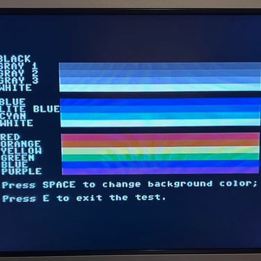
The basic functions of the VIC-II, SID and RAM is tested with 64 Doctor. Note that this is to be considered as basic functionality - more advanced (?) functionality such as sprite handling / collision detection / advanced audio will be tested later. But the basic tests pass without any detected faults (click to enlarge).
Extended testing
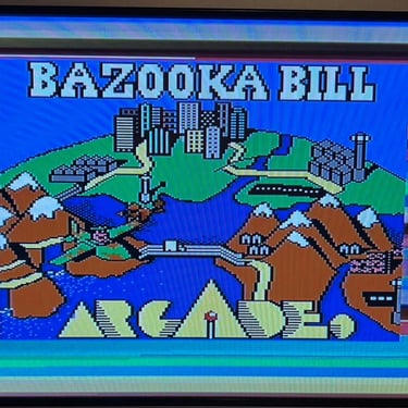
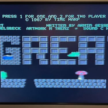
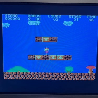
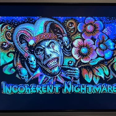
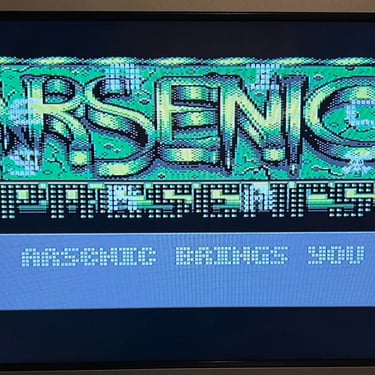
Knowing that the basic functionality of the machine works I continue the testing by using the Commodore 64 for normal operations; playing some games, watching demos, loading from datasette and floppy and using a cartridge. I can not find any issues with this machine. I also pay special attention to the video to make sure that there are no glitches in the graphics - I can´t see any abnormalities. Below is a gallery with pictures from the testing.


Final result
"A picture worth a thousand words"
Below is a collection of the final result from the refurbishment of this C64. Hope you like it! Click to enlarge!
Banner picture credits: Evan-Amos