
C64 Breadbin [PAL]
(Converted from NTSC)
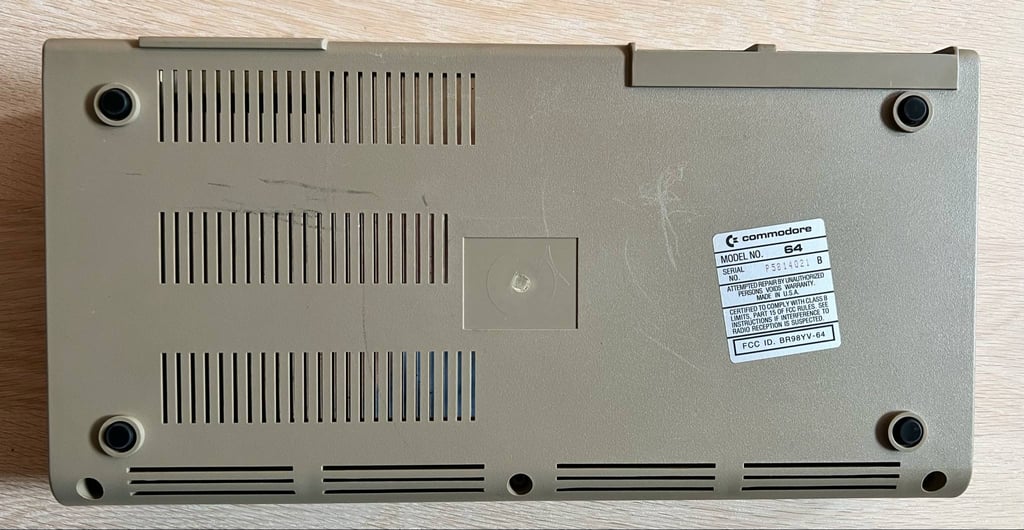
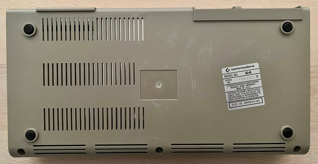
Ser. No. P5814021
Assy 250425
P/N 251470-01 (REV A)
Starting point
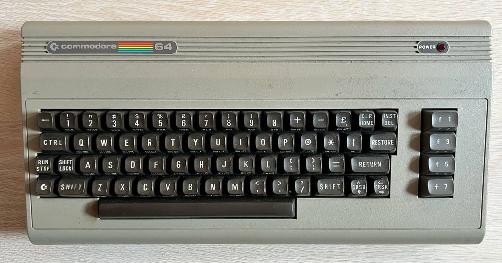
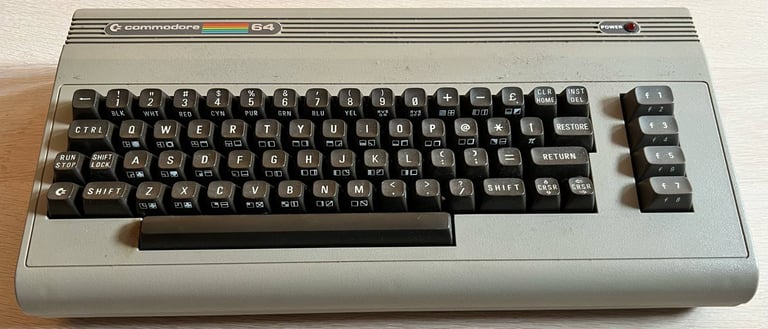
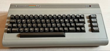
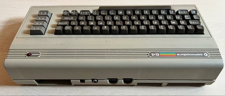
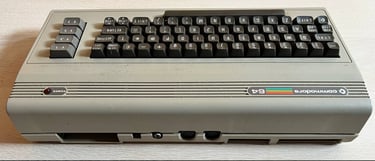
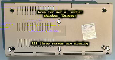
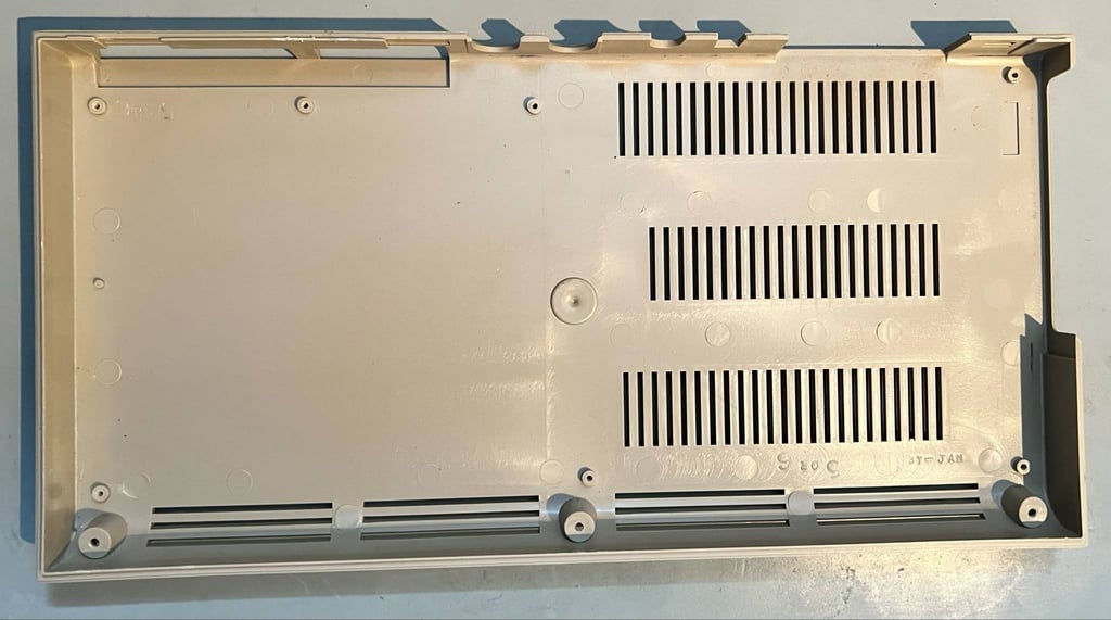
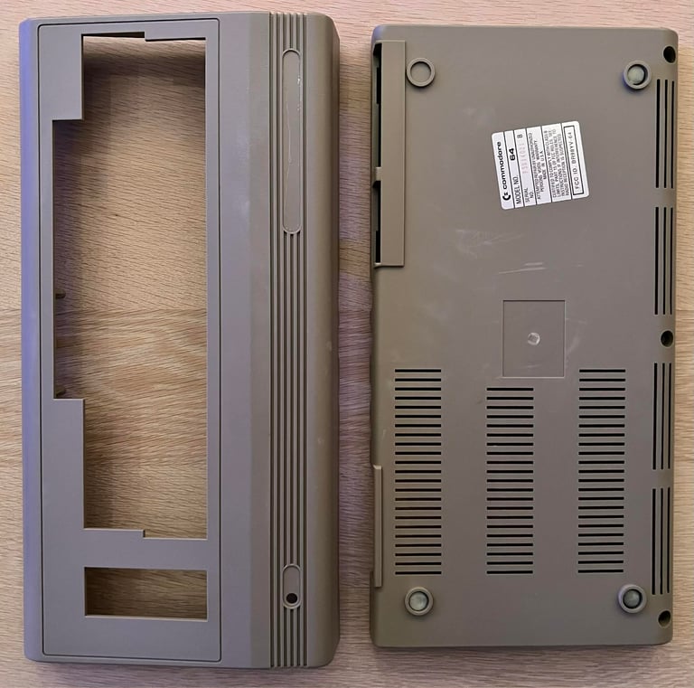
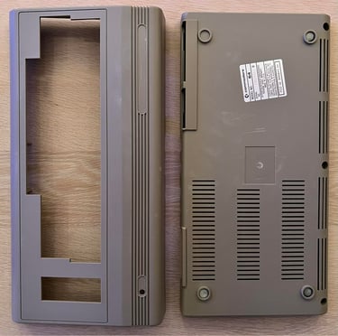
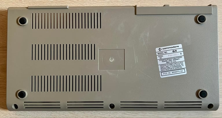
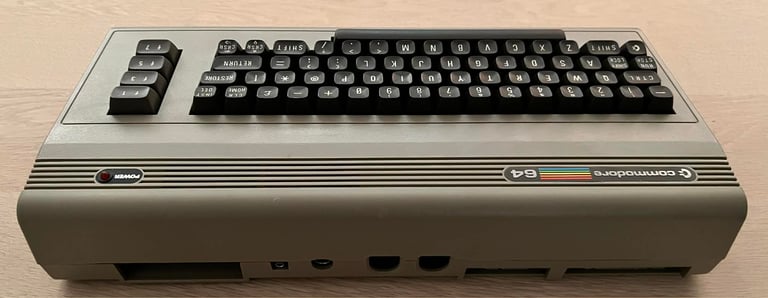
This Commodore 64 is in for some refurbish, and probably some repair. From the outside it is very dirty, but it appears to be most old dust and grease. The machine seems to be mechanically OK with to immediate signs of broken or not working parts. Since all the three screws at the bottom cover are missing, the whole top cover is loose.
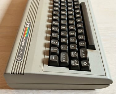
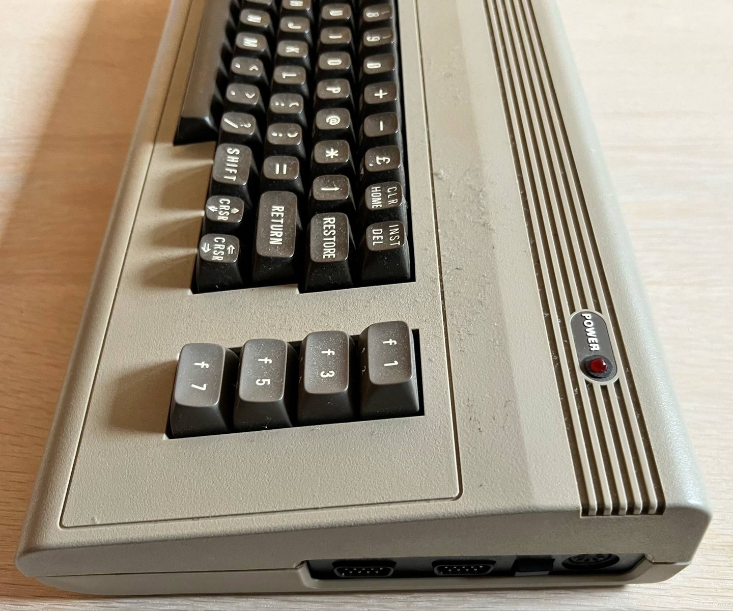
I also notice from the serial number label that this is probably a NTSC machine: the label is not placed in the "label area" due to its size, the label refers to FCC compliance and the serial number structure itself is different from PAL machines.
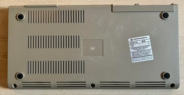
Below are some pictures of the Commodore 64 before refurbish.


Refurbishment plan
The refurbishment plan for this C64 breadbin (several of them in parallell):
- Refurbish the casing (cleaning, repairing and retrobrighting)
- Refurbish the keyboard (cleaning, reviving the plungers and potentially retrobrighting)
- Refurbish main board (cleaning, checking, repairing, replacing capacitors and voltage regulators if required, adding heat sinks etc.)
- Verify operation by testing
The plan can be updated during the refurbishment process. Sometimes I discover areas that needs special attention.
Disassembly
Disassembling the covers and PCB
The first step of disassembly is very easy. There are no screws - so it is just a matter of lifting the top cover from the bottom. Note: when lifting a top cover on the Commodore 64 it is good practice to lift it only 30 degrees first and then wiggle it loose. This will reduce the probability of braking the rear tabs. Also, notice how the serial number sticker is not placed on the "normal" center spot (for European machines) due to the US sticker size (showing FCC compliance).

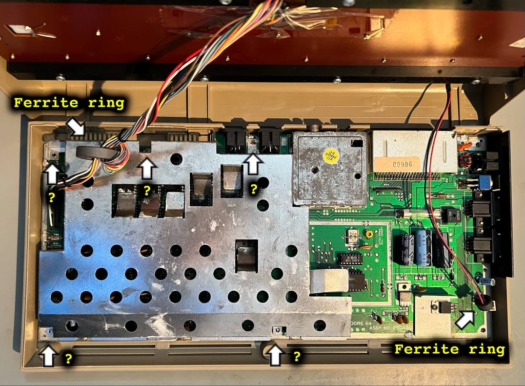
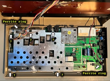
Lifting the top cover the interior is revealed. There are some things to notice:
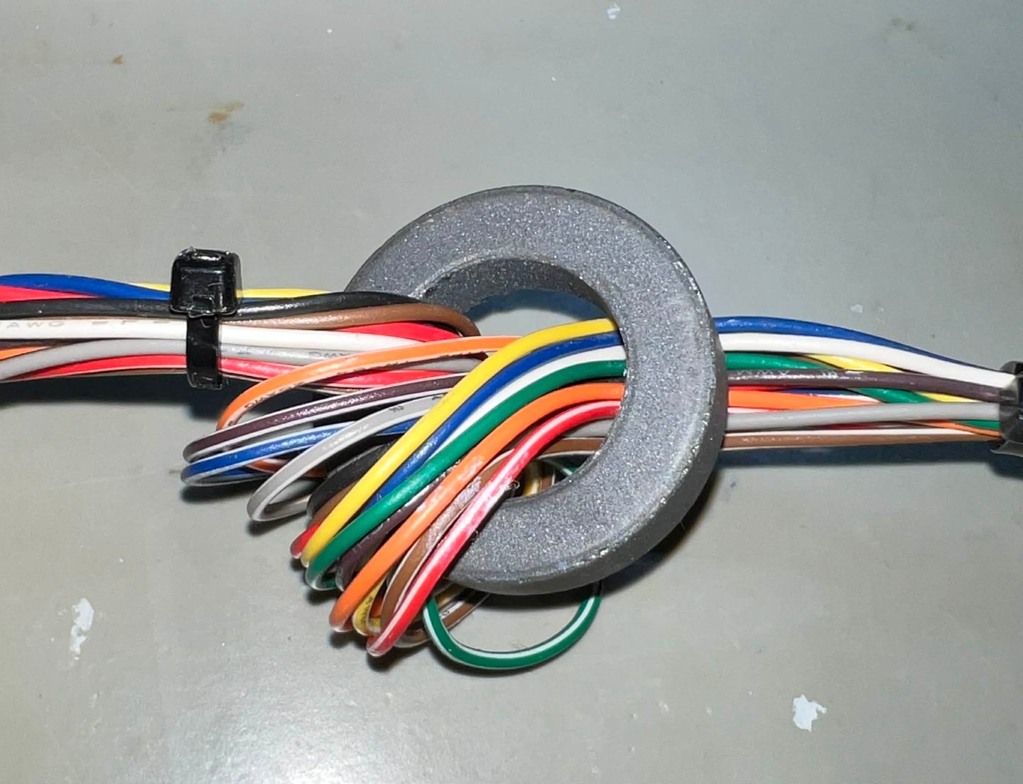
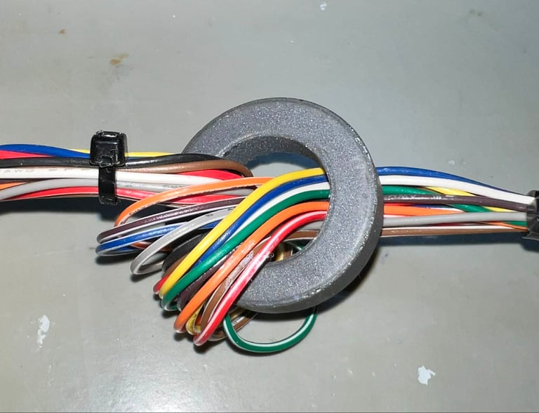
There is another indication that this is a NTSC machine. There are ferrite rings surrounding wires (both from the keyboard and LED) which is typically to comply with FCC regulations
None of the PCB screws are present
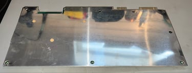
The RF shield looks a bit dirty, but I think that its just a matter of some proper cleaning
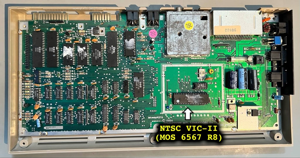
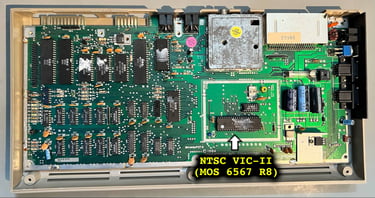
The RF-shield, which also function as a heatsink, is simply lifted from the PCB since there are no screws holding it in place. The complete PCBA is now revealed, and now there is no doubt: this is a NTSC Commodore 64 equipped with the MOS 6567R8 VIC-II.
Again, no screws holding the PCBA to the bottom cover. The whole PCBA is simply lifted out of the bottom cover which looks to be in good condition.
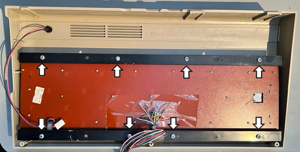
Removing the keyboard and LED
The keyboard is mounted to the top cover with eight 3.5 x 9 mm Phillips screws which are removed.
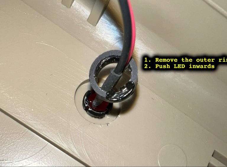
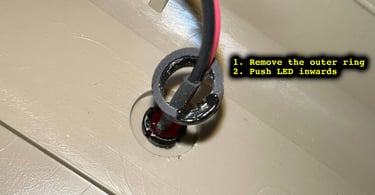
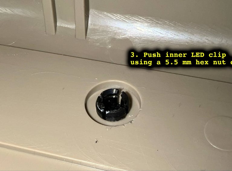
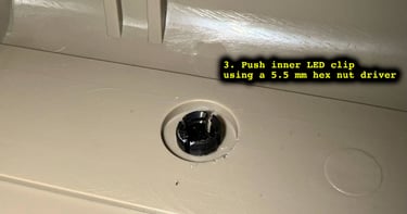
Removing the LED is not complicated, but can be very easy if you follow these steps:
Remove the outer ring surroundind the LED wires with a flat thin screwdriver. This will loose easily by prying it off.
Place the top cover firmly on the table top resting only on the tip of the LED. With a firm press on the top cover (now with the LED pressing on the table top) the LED will pop out
With a 5.5 mm hex nut driver the inner LED clip is pushed out (from the inside of the top cover towards the outside)
NOTE: The inner plastic ring is a bit damaged for unknown reasons.
Casing
As previously mentioned the casing is very dirty. There is literally dirt and grease all over it.
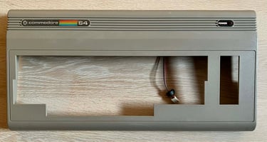
Removing the metal badged
Before the casing is cleaned, the "Commodore 64" and "Power" badge are removed. NOTE: these badges will likely be transferred to another C64 machine since this will be refurbished first (and I´ll get new badges for this later).
The trick to remove the badges without damaging them is to apply some hot air from a hairdryer - and at the same time carefully pry the badges off with some prying tools. Both badges are removed without any damage to either casing or the badges themselves.
Cleaning the casing
Both the top- and bottom cover are placed in mild soap water for about a week (together with another C64). This will dissolve most of the dirt and grease.

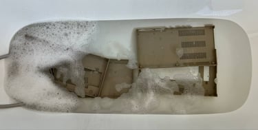
After the long bath, and with some isopropanol to remove the last stains, the covers looks way better!
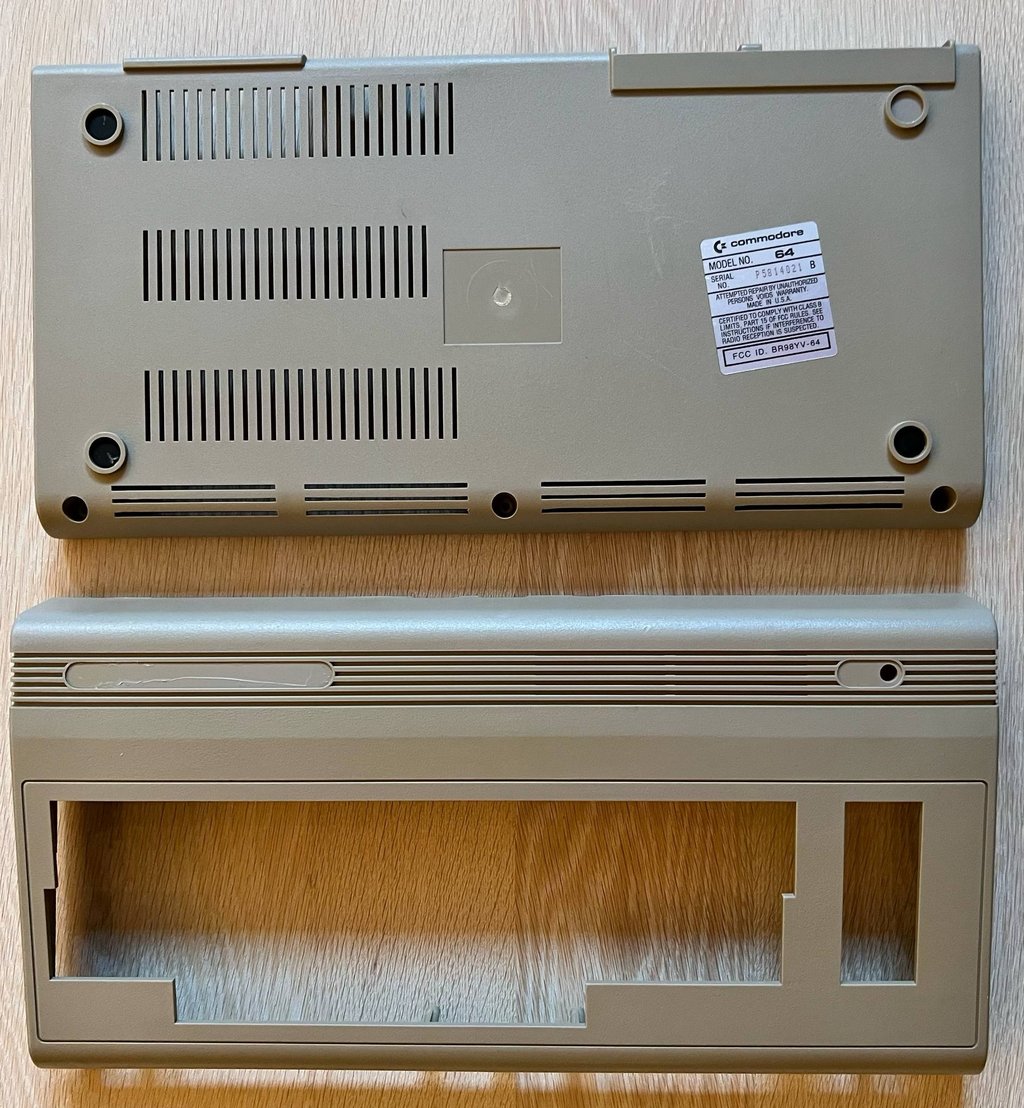
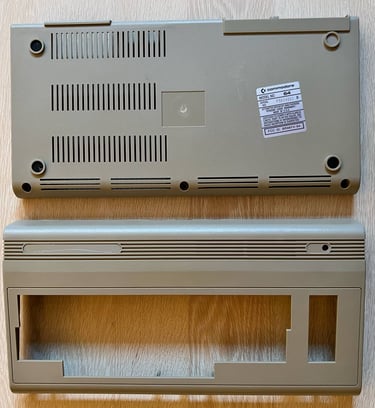
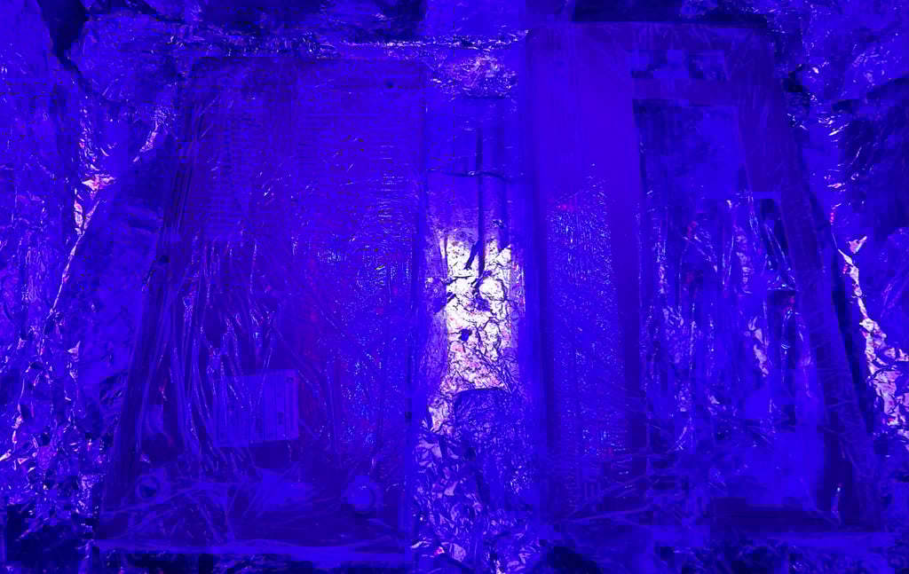
The covers are not severely yellowed, but I still think that it is worth the effort of retrobrighting. So the covers are retrobrighted for about 12 hours straight using 12 % hydrogen peroxide cream on the covers while exposed to UV light.
After the retrobrighting the covers look better. Yes, you can argue that the retrobrighting has made some of the scratches (at the bottom cover) more visible, but in total I think the result is good. There are some marks from the retrobrighting, do doubt, but I do think they look also better in reality than in the pictures.

NOTE: the "Commodore 64" metal badge is transferred from a spare machine (incidentally made in the USA also) with serial no. CA4037506.
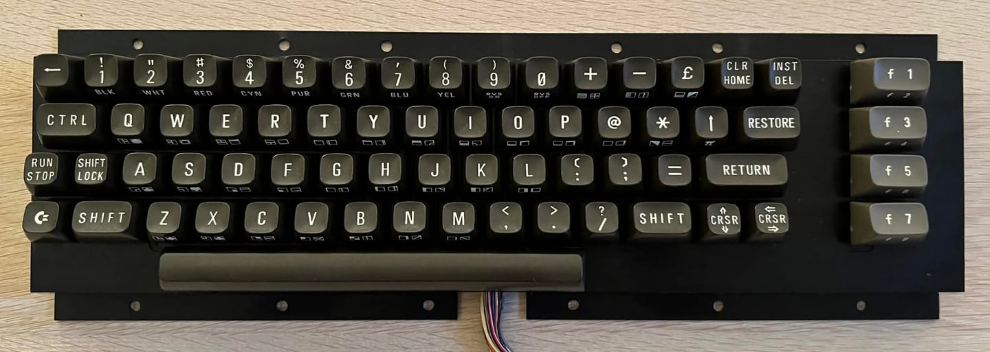
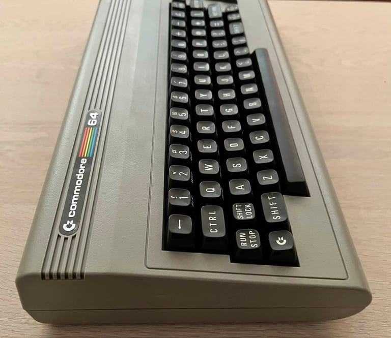
Keyboard
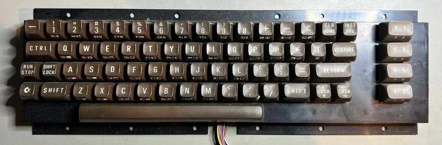
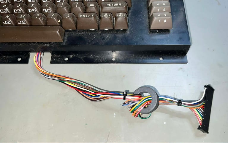
This is a fine looking keyboard. Yes, it is a bit dirty and slightly yellowed, but otherwise it appears to be in good condition. Also, notice that there is a large ferrite ring surrounding the keyboard wires with the purpose to suppress noise. This is something not seen in European Commodore 64s (PAL) as far as I know, only the US version (NTSC) have this ferrite ring. Below are some pictures of the keyboard before refurbish.


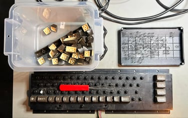
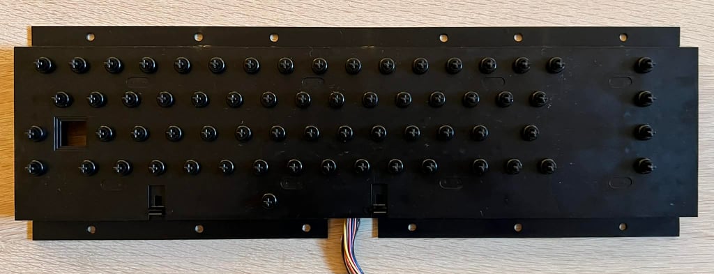
A detailed description on how to refurbish the keyboard can be found here. First, all the 66 keycaps are removed using a keycap puller. There are small springs beneath each of the keycaps. Note that:
There is a larger spring beneath the SPACEBAR so it is good practice to keep this in a separate bag while refurbishing
There are no spring beneath the SHIFT LOCK keycap (this is normal)
There are some dust and grease under the keycaps which is expected. But there is significantly less than I have seen on other Commodore 64s. My assumption is that this machine has not been very much used, and also stored in a proper placed.

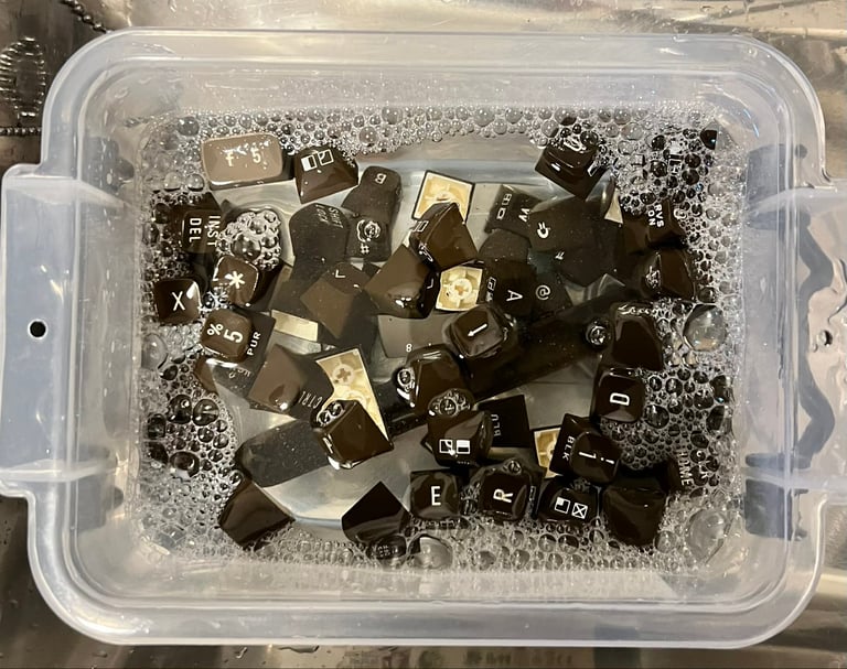
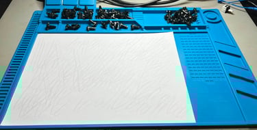
All the keycaps are placed in a box filled with mild soap water for about 24 hours. This should remove most of the dust and grease from the keycaps.

To remove the PCB from the keyboard all the 23 small screws at the backside are removed. But before that is done, the SHIFT LOCK is desoldered. There are two uninsulated wires soldered to the SHIFT LOCK key.
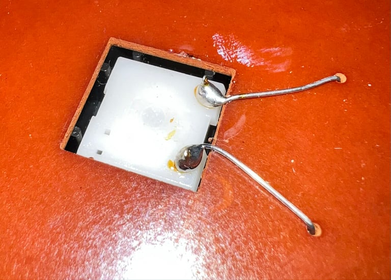

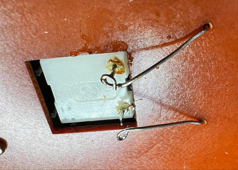
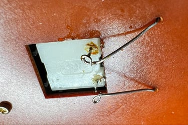
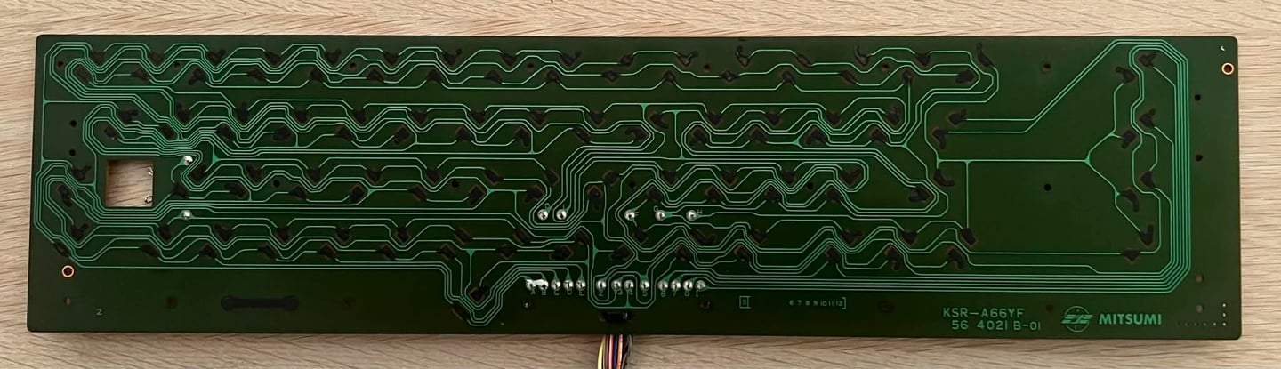
The keyboard PCB is from Mitsumi and is version "KSR-A66FY 56 4021 B-01". This is the "B" version with carbon pads. To make sure the carbon pads are not damaged the PCB is cleaned with only distilled water.
An effective, and simple, way to revive the plungers is to gently rub the conductive rubber on a clean sheet of paper. This will remove most of the dust and grease on the conductive rubber - reviving the plungers.

The plastic frame is cleaned properly with lukewarm mild soap water. After drying the plungers are put back into the plastic frame and the keyboard PCB is mounted back. The result is very nice - good as new.
After cleaning, and drying, the keycaps they are put back on the keyboard. The keycaps are as mentioned slightly yellowed on the top side of the keycaps, but looks otherwise very good.
Mainboard
Visual inspection
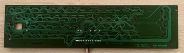
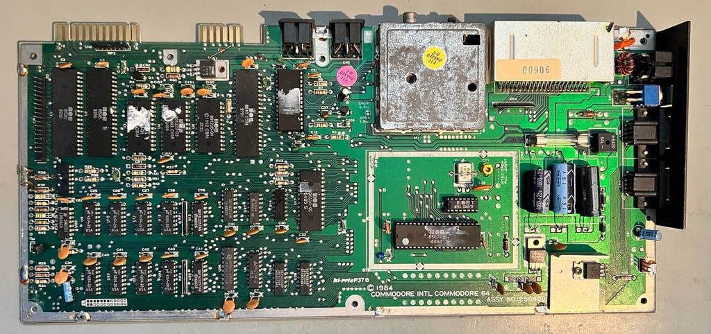
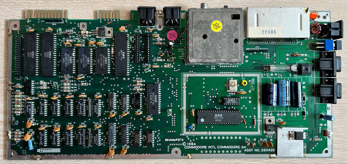
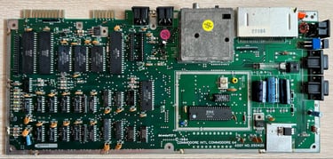
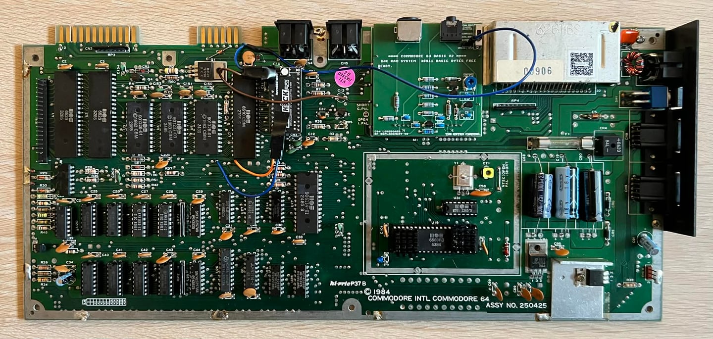
This is an Assy 250425 mainboard 251470-01 Rev A (PCB also marked with "Hi-Pric 37A"). A quite common mainboard found in mid-age Commodore 64 breadbins. Unfortunately, I am aware that these PCBs can be challenging to work with due to poor PCB quality (ripping pads and traces due to desoldering). But hopefully we will not have too much of a problem here.
Since this is a NTSC mainboard there is a large RF-shield covering the backside of the mainboard to comply with US FCC regulations. This is something you do not see on PAL machines for the European market (as far as I know).
The mainboard looks to be in overall good condition. First thing I notice is that all the thermal paste, both for several custom ICs and VR2, has completely dried out. This needs to be cleaned and replenished later. Naturally, there are some dust and grease and some oxidation/corrosion on RF-modulator, user-, datasette-, and cartridge port. But otherwise I can not see any major damage, bulging/leaking capacitors, broken traces/pads or re-work. Also, there are no screws holding the metal plate covering the control ports and power socket.
Below are some pictures of the mainboard before refurbish.

In the table below all the custom ICs are listed. And as can be seen from this table is that all original ICs were produced between week 48 of 1985 to week 05 of 1986 so I think we can assume that this Commodore 64 was produced in the autumn of 1985.
Initial testing
An initial test is performed on the mainboard. This is done with the purpose of checking the initial status of the mainboard - checking for any fault symptoms. In the table below the result are shown.
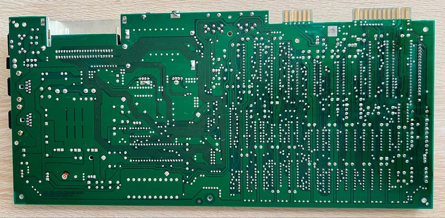
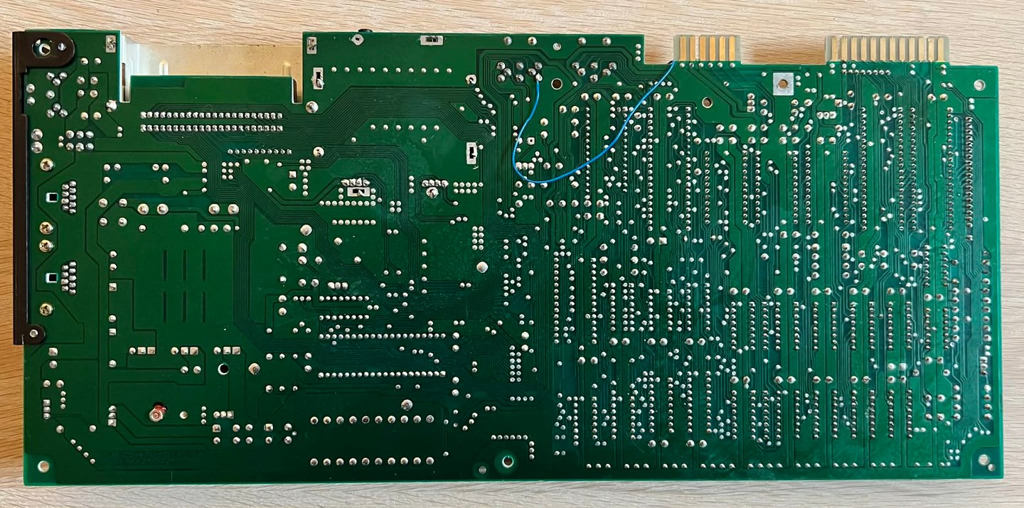
Removing the bottom RF-shield
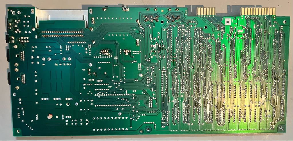
Since this is a NTSC machine there is a RF-shield covering the backside of the PCB (to comply with US FCC regulations). To remove this shield all the soldered metal tabs needs to be desoldered and bent. This RF-shield will probably not be put back after refurbish as it has no (or marginal) function now.
Below is a picture of the backside of the PCB with the RF-shield removed. I notice that there are quite some flux residue, but this is to be expected.
Cleaning the mainboard
Before the repair, and refurbish, continues the mainboard is cleaned. This is done by first removing the socketed ICs (and the fuse), and then washing the mainboard with mild soap water and a paint brush. After cleaning the mainboard is left for drying for a couple of days. Below are some pictures of the mainboard after cleaning.
Checking the voltages
For the Commodore 64 to work flawlessly all the different voltages need to present and within acceptable tolerances. A detailed article on the subject can be found in the HOWTO - Checking the C64 voltages. In the table below all the measures voltages are listed (this list will also be updated after refurbishment). All the required voltages are present and within tolerances, so there are nothing obvious wrong in that area.
Mainboard - Repair
Faults investigation
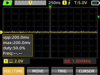
After some checking with the oscilloscope I notice something. There are no AEC signal coming from the VIC-II. This is a very important signal as it will then when the CPU and the VIC-II are to operate on the data- and address bus. And this signal should be generated by the VIC-II I believe. Well, there is a signal, but it is incredible small. Just a flat signal about 0.2 V (measured at PIN#16 on the MOS 6567 VIC-II). See picture below.

Converting from NTSC to PAL frequencies
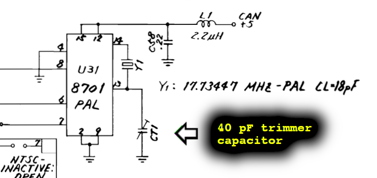
Before continuing the repair, the machine is converted from using NTSC frequencies to PAL frequencies. The schematics describing the clock circuit is shown in the picture below (taken from schematic #251469 in the C64 service manual).
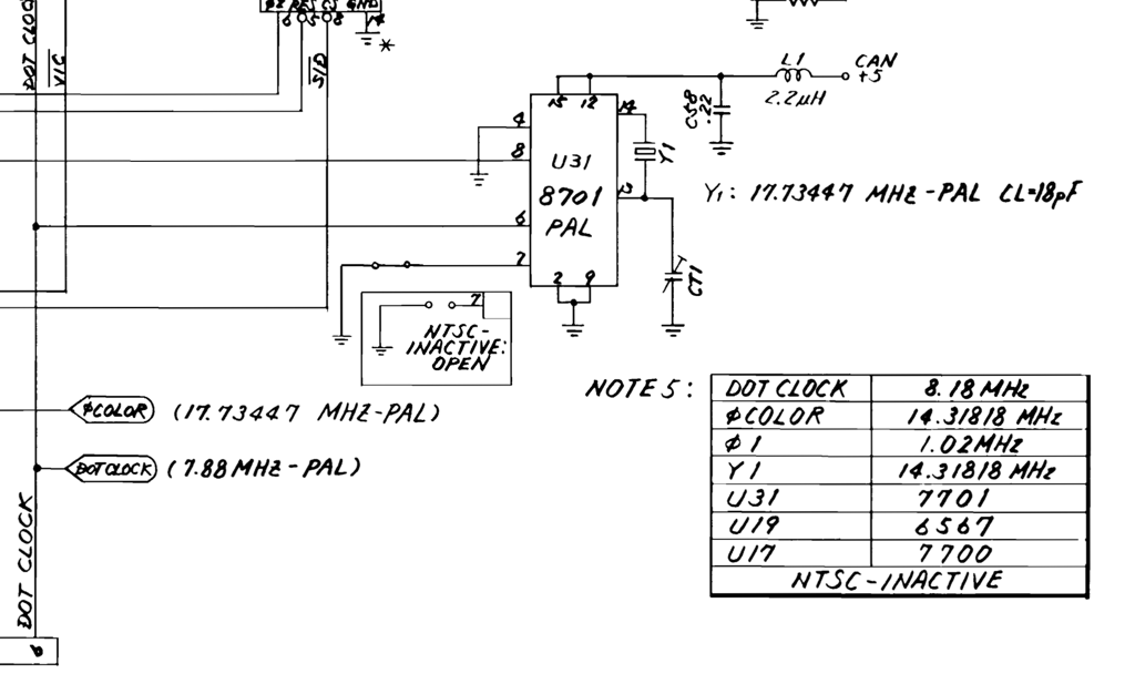

This schematic from the service manual also shows something interesting. On the bottom right hand side of the schematic there is a table showing the NTSC frequency values and the ICs used in a NTSC machine. Notice especially U31 and U17 which refers to MOS 7701 (CLOCK) and MOS 7700 (PLA) respectively. Why? This very machine is a NTSC machine but does not use any of these - instead it already use the MOS 8701 (CLOCK) and MOS 906114-01 (PLA) found in PAL machines. I think it is a fair assumption that earlier versions of the NTSC machines did use the specialised (?) NTSC ICs, but that these were replaced with PAL ICs at some point.
As can be seen from the schematics above there are two things required to switch from NTSC to PAL frequencies:
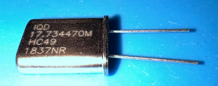
Replace the Y1 crystal. From a 14.31818 MHz to a 17.73447 MHz crystal.
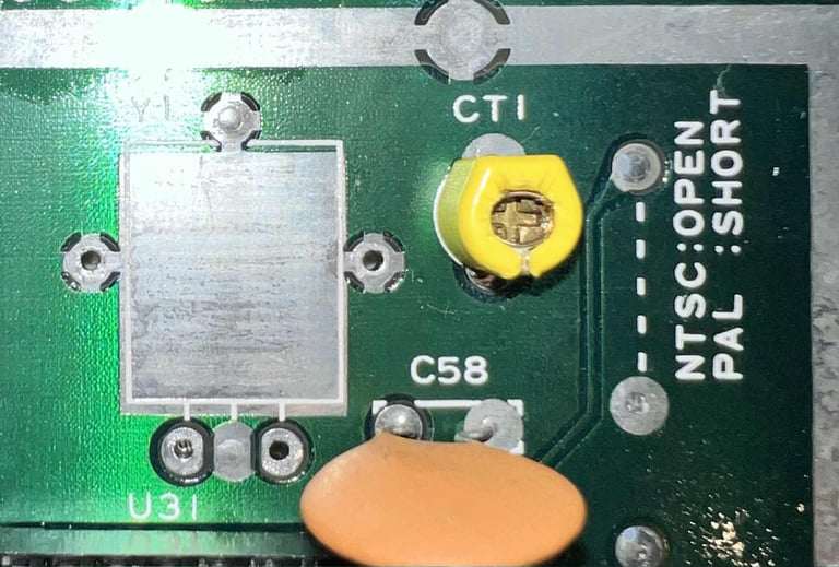
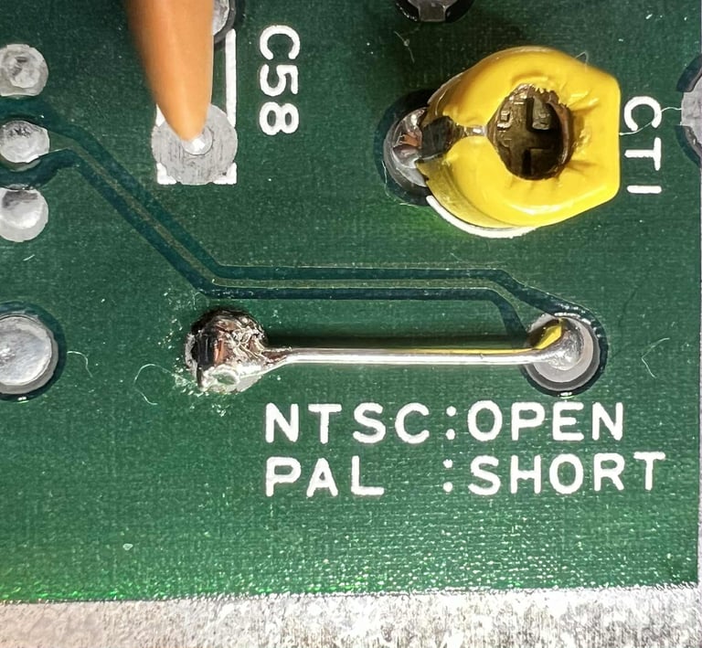
Close the "NTSC-INACTIVE" jumper
Before any changes are done the current NTSC frequencies are measured. This is done to confirm that they match the frequencies put forward in the table in the schematics above.
[*] Instability in frequency measurement is likely caused by the handheld oscilloscope not able to accurate trigger high frequencies.

A new Y1 crystal with oscillation frequency of 17.73447 MHz is soldered in (the crystal is sourced from Mouser).

Finally the "NTSC-INACTIVE" jumper is closed with a small wire.

After installing the new Y1 crystal the frequencies are measured again.
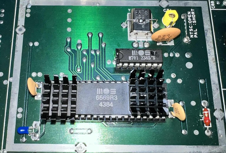
There is still no activity on the AEC line (pin #16 on the MOS 6567 VIC-II) so I suspect that his IC is dead unfortunately. A "new" PAL MOS 6569 VIC-II is installed on the mainboard (note that this IC has already some heat sinks on each side of the chip. If this IC fix the problem a heat sink will also be placed in the the center of the IC since this is where the heat is generated).
The old Y1 crystal is desoldered from the mainboard without any damage to tracks or pads.
[*] Instability in frequency measurement is likely caused by the handheld oscilloscope not able to accurate trigger high frequencies.

The machine is powered on and the AEC signal on pin #16 is measured on the new PAL VIC-II chip. And now there is a proper signal there! The AEC (Address Enable Control) is directly connected with AEC of the CPU. When going LOW, the CPU puts its bus lines into high impedance state and is thus totally decoupled from the rest of the system, so that the VIC-II can take control over it.

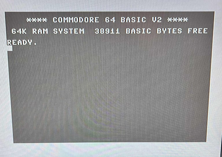
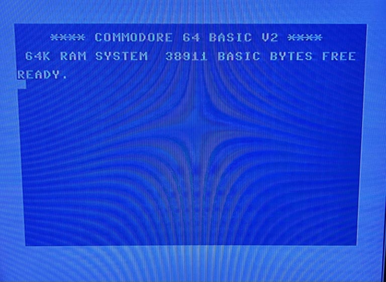
Does the machine work now? Well... not quite. The machine do start with proper startup screen (38911 BASIC bytes free) which is really nice, but there are no colour! The screen is black and white.
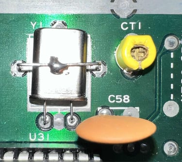
The black and white screen is probably caused by a slight misalignment in frequency after the new Y1 crystal was installed. A 40pF trimmer capacitor, CT1, can be used to adjust this. See schematic below.

It turns out that it is not easy to adjust the trimmer capacitor. When using a small screwdriver to adjust the capacitance, the component gives a terrible grinding sound! Some contact cleaner does help a little, but not much. So, a spare trimmer capacitor is installed. Desoldering the old trimmer capacitor - and installing the new one is done without any damage to traces or pads.

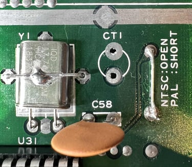
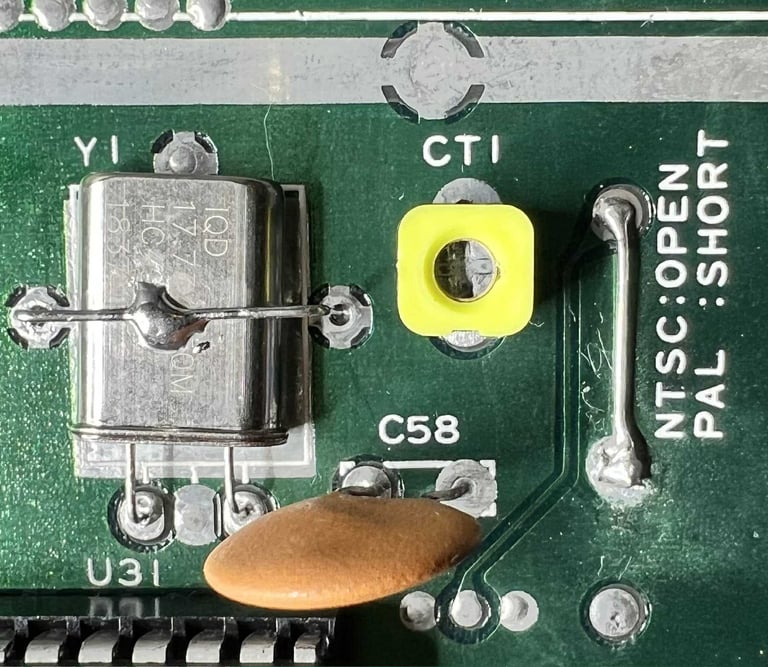
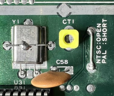
With the new trimmer capacitor (CT1) in place the color is back (after a small adjustment on CT1 with a screwdriver).
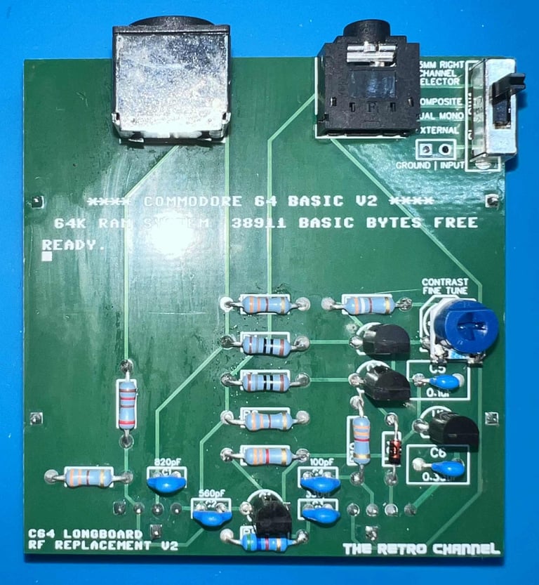
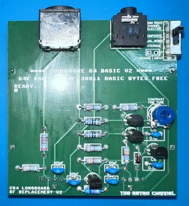
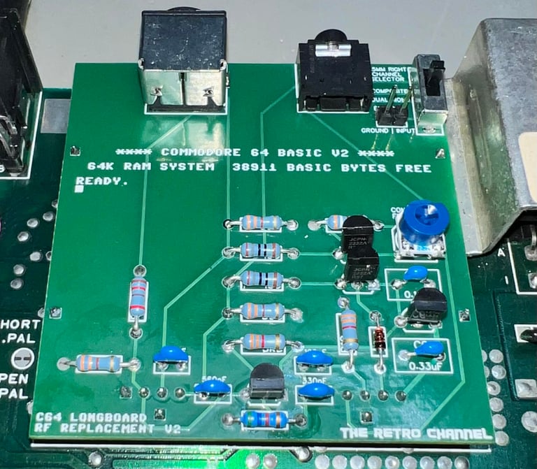
Replacing the RF-modulator
"There is a new RF-modulator in town..." - The original RF-modulator does not provide the best video output possible. To fix that The Retro Channel have made a modern replacement: Commodore-64-RF-Replacment-Longboard-V2.This module will provide not only a better video quality, but also:
Superior video output compared to the original RF modulator
Direct S-Video output for S-Video capable displays and upscalers
Optional HDMI (DVI) output for the large VIC-II Kawari
Adjustable luma:sync ratio (contrast control)
Signal passthrough to the C64 AV DIN - for those who prefer to use the standard DIN connector
3.5mm stereo audio output with the left channel dedicated to SID audio, and right channel selectable between SID audio (dual mono), composite video, and external (for dual SID setups, LumaCode, etc.)
The RF-modulator is assembled by me following the instructions from The Retro Channel. Below is a picture of the assembled module.
Removing the old RF-modulator is not trivial. It is not that it is hard, but if you are not very careful you risk damaging pads, traces and the RF-modulator itself. If you are curios on how to remove the RF-modulator please have a look at the HOWTO article: Desolder the RF-modulator.
The RF-modulator is desoldered without any damage to traces or pads. See picture below.

Finally the new RF-modulator replacement is soldered to the mainboard.

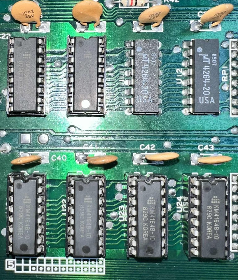
Replacing the 8 x MT RAM ICs
Replacing all of the working RAM IC? Yes. The Micron Technology (MT) 4264-20 RAM ICs are notorious for failing. So, even if they are working fine now I choose to replace all of them with new RAM chip, and also install sockets for the ease of future service. The new RAM ICs are Samsung 4164B-10.
But now something odd happens. When the sixth RAM IC is installed the machine stops working. Black screen! What happened? Did something break during the operation? I can not find any broken trace or pads, but there is obviously something wrong.
Below is a picture of the mainboard with the six RAM ICs installed. I will repair the machine before continuing replacing the last two RAM ICs.
Faults investigation
The symptoms after installing the 6th RAM IC is:
Black screen, but video signal (black)
No response from Dead Test Cartridge
So, what could be causing the sudden black screen? The most likely would be a bad/broken connection, or a short circuit, related to the 6th RAM IC. Since the machine worked fine up til the 5th RAM IC. But no fault of this kind is identified.
With the oscilloscope some vital signals are measured, and there is one signal which does not look correct at all:
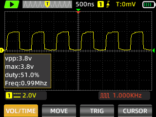
The /RESET signal on PIN#40 on the MOS 6510 CPU is not set to HIGH after a short while. Instead a square wave, with frequency about 6 kHz, is measured which is not correct. See picture below.

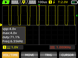
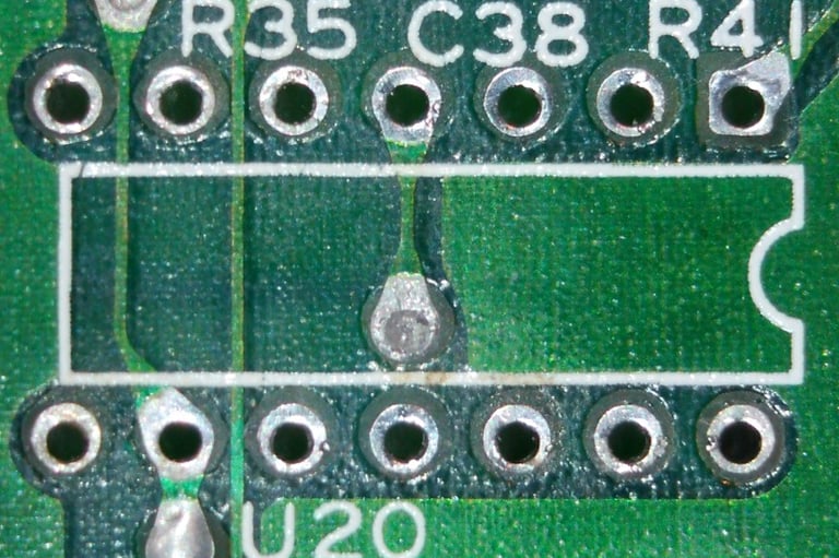
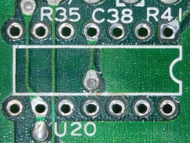
The same square wave (but inverted) can be found on PIN #9 on the 556 timer circuit (see schematics below).

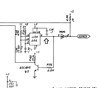
Replacing the LM 556 timer
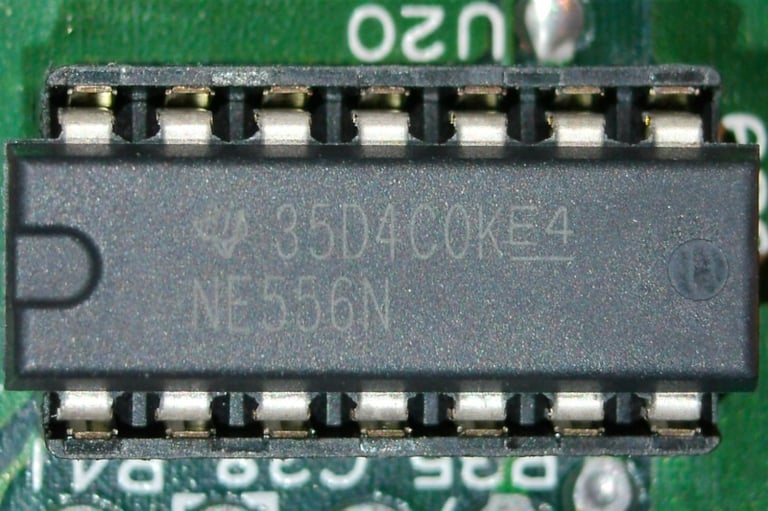
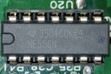
It appears that the LM 556 timer is causing the RESET line to pulse at 6 kHz - could the LM 556 be bad? So the LM 556 (U20) is desoldered. The desoldering is done without any damage to traces or pads, a socket installed and a NE556 replacement is installed. The NE556 should be interchangeable with the LM556. See pictures below.
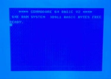
With the new 556 timer in place the machine is powered on. RESULT: Success! The machine boot up to the good old blue BASIC screen with 38911 BASIC BYTES FREE. Although, it feels that the machine takes a bit longer to restart. Maybe the NE556 has slightly different timer specifications? No that it matter in any way.
Replacing the 8 x MT RAM ICs - continued
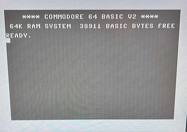
After the 556 timer is replaced, and the machine is working again, the remaining two MT RAM ICs are desoldered and replaced with new Samsung 4164B-12 ICs. Note that these are slightly different with the -12 instead of the -10 on the other. This should not make any difference. With all the eight RAM ICs replaced the machine works fine. The machine boot to 38911 BASIC BYTES FREE.
An analog fault?
Did you think that we were out of the woods now? Oh no... a few hours after the RAM ICs were replaced the machine now shows no video output at all. It is not even a black screen. It is completely black - no video sync at all.
What on earth happened now?
Troubleshooting
First thing to check is to validate that there actually is no signal (S/LUM) on pin #15 on the VIC-II. And there is not. No signal at all. Completely dead. A known good VIC-II is installed to see if that helps, but to no avail. The S/LUM signal is still gone even with a known working VIC-II.
Next thing to do is to check the Phi color clock and Phi dot clock on pin #21 and #22 respectively. These two signals are required both for generating the CPU clock and the S/LUM analog video signal. But both these signals are present and they look as they should according to the reference signals.
And as a matter of fact, all the signals on the VIC-II chip appears to be as they should - except the S/LUM signal on pin #15. What could cause this?
But now I notice something interesting: when the MOS 6569 VIC-II is not installed in the socket, and the voltage on pin #15 in the socket is measured, the voltage seems to be too low: approximately 2 V. I was expecting this voltage to be higher (3-5 V area) in order to be able to pull-up the S/LUM signal. Currently my hypothesis is that there is something wrong with the RF-modulator replacement.
Validating that this is an analog fault
Even if there are output no video signal, a simple test is done to validate that the machine is actually working (seen from a digital perspective). The test is done by connecting the keyboard to the machine and typing "SYS 64738". This will perform a cold reset on the machine. To do this without any video display the oscilloscope is connected to the /IRQ line (here: pin #21 on CIA#1). When typing the "SYS 64738" and then pressing RETURN (in the blind) the /IRQ will stop for a short while during the reset. This should be a proof that the machine is actually working - even if it does not display any analog video output.
In the video below you can see how this looks when then the SYS 64738 is executed.

Identifying the culprit?
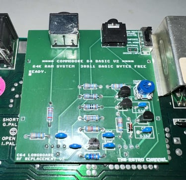
During the troubleshooting there is something I notice: the 7805 +5V voltage regulator (U1) located in the RF-replacement module does not output +5 V DC. See picture below.

There are no short to ground on the output pin, so it is likely that the 7805 voltage regulator is faulty. So, the RF-modulator replacement is removed and a 2nd RF-modulator (same as the one already installed) is soldered in place.

With the new RF-modulator in place the machine is powered on again. And, SUCCESS! The good old blue screen showing 38911 BASIC BYTES FREE is back. With a multimeter the output on the 7805 voltage regulator is checked now and it shows 5.02 V DC. Nice!
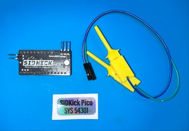
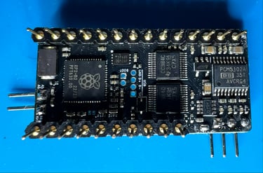
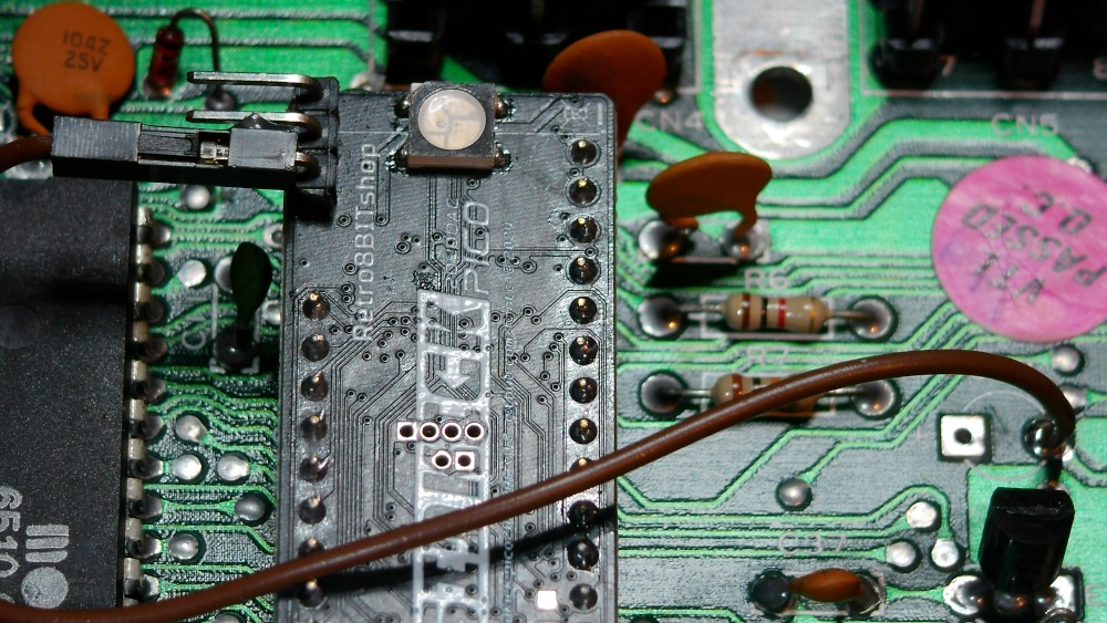
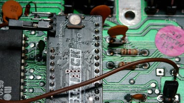
SIDKick Pico 2040 ADC
Since the original SID was transplanted to another Commodore 64 during a previous repair a great replacement is installed: the SIDKick Pico 2040 ADC. From the SIDKick Pico GitHub page we can read:
The SIDKick pico ("SKpico") is a drop-in replacement for the SID 6581/8580 sound chips in the Commodore 64 and 128 computers, and it can also emulate the SFX Sound Expander (FM).
The emulation is based on an extended version of reSID 0.16 (with parts from reSID 1.0 plus some extras), and also includes a few unique features:
dual 6581 and/or 8580 emulation, or 6581/8580 plus FM emulation
advanced SID filter settings plus 19x measured 6581 filter curves
2nd-SID address at $d400, $d420, $d500, $d420 + $d500 simultaneously, $de00, $df00 (on C128 no $d500), or any address when an external chip select signal is used (e.g. for the C64 Ultimate or on Ultimate 64 boards)
paddle/mouse support with optional anti-jittering
built-in configuration menu (launch with "SYS 54301"/"SYS 54333", also from C128-mode)
built-in PRG launcher ("SYS 54333,0" etc. or from the menu), PRGs can be integrated into the firmware or flashed from the configuration menu
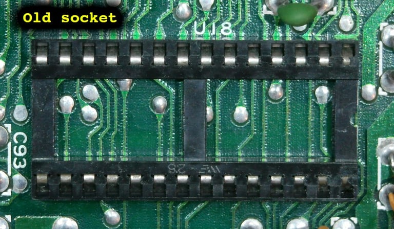
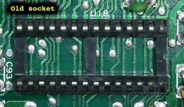
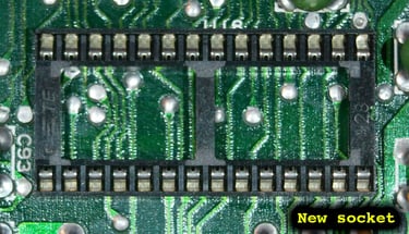
Replacing the old U18 socket
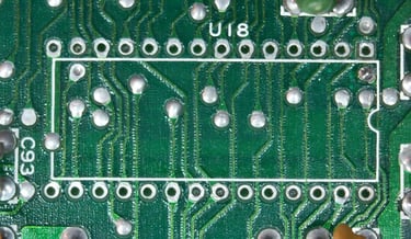
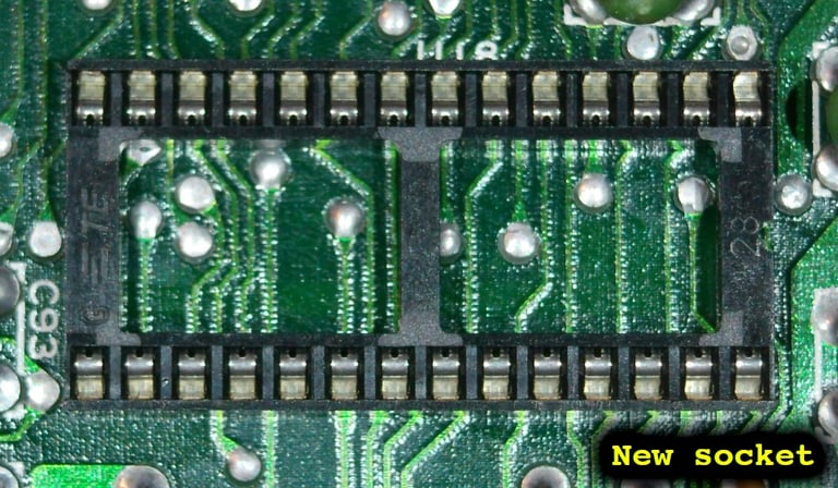
To install the basic configuration of the SIDKick Pico 2040 ADC is straightforward: just insert it in the U18 socket. But on the first try of the SKPico I get no sound. Pressing the SKPico down in the socket I do get sound on the second try. This leads me to think that the old U18 single-wipe socket is worn out. So the old socket is desoldered, and a new dual-wipe socket is installed. No traces or pads were damaged during the desoldering/soldering.

Even with a new dual wipe socket I did manage to see that the SIDKick Pico did not start up. But I noticed some odd looking solder joints on the the SIDKick Pico PCB which I resoldered. I will keep an eye on the situation, but for now it seems to work just fine.
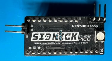
The SIDKick Pico 2040 ADC kit also contains a nice sticker with the SYS 54301 (for the config menu) and two grab wires with Dupont connectors. Below are some pictures of the kit before installed in the Commodore 64.


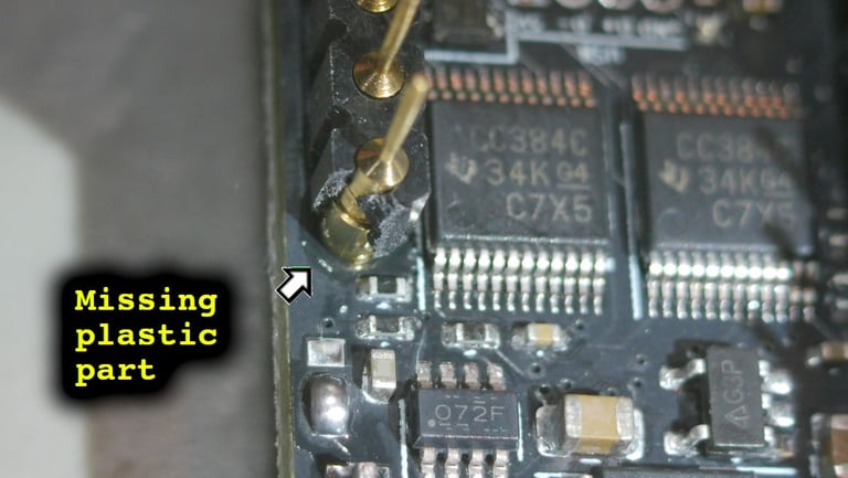
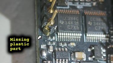
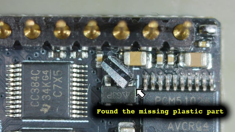
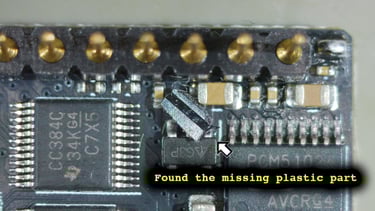
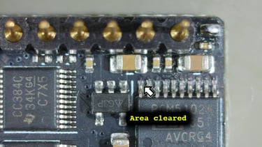
Noticing a small crack
When cutting a row of pin headers it sometimes happens that parts of the plastic breaks. And so is the case here. This has probably happened during assembly before I received the assembled device). Nevertheless, it is good to be aware of. Below are some pictures taken with the microscope. As a matter of fact I managed to find the broken plastic piece actually still "stuck" on the PCB.
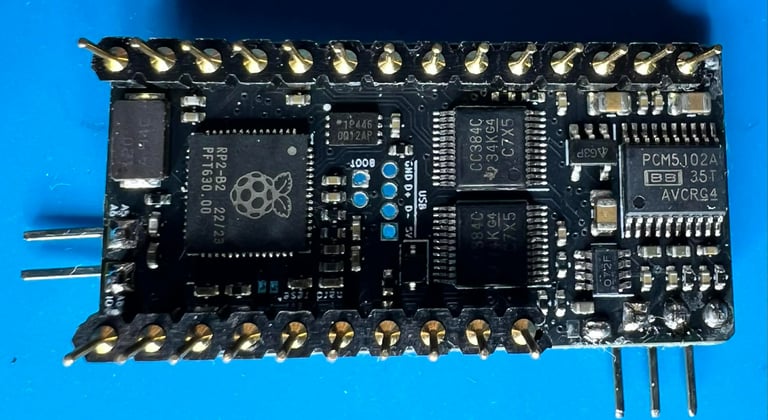
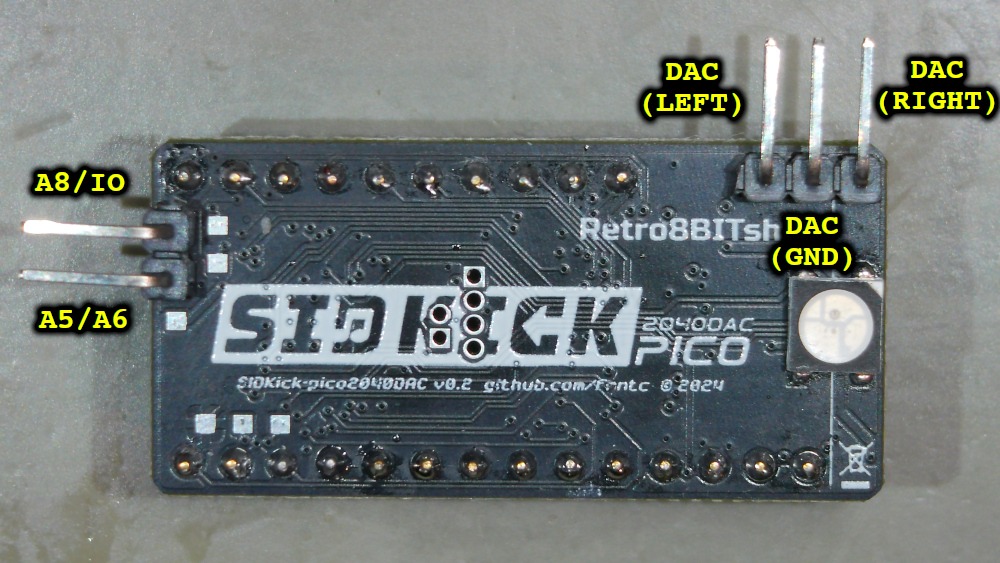
PINOUT
There are five pin headers on the SIDKick Pico 2040 DAC. Two of these are used for addressing lines >A4 and three are used for analog audio output. See picture below.

Ok, so what is the plan?
Well, the SIDKick Pico 2040DAC is quite a magnificent piece of hardware. It is not only a 1:1 SID replacement. So the plan is this:
Make the 2nd SID available by adding, and soldering, required wires to the address bus
Utilise the Digital-Analog-Converter (DAC) which makes a far better audio output:
Disable the old original PWM audio signal to PIN 3 on the A/V connector and instead use the DAC signal (LEFT)
Route an additional wire with DAC signal (RIGHT) to PIN #7 on the A/V connector. This will make STEREO available also from the A/V connector.
Route both the DAC signal (LEFT and RIGHT) to the new RF-modulator replacement to enjoy STEREO audio via the 3.5 mm TRS plug.
Add some PRG files to the SIDKick Pico chip for easy access
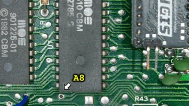
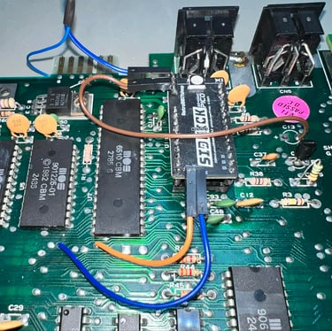
Connecting the A5 and A8 address line
The original SID chip only use address line A0-A4. But the Commodore 64 memory map shows that the reserved I/O map for the SID is from $D400 - $D7FF. With only the address lines A0-A4 the stock SID cannot see any difference between addresses such as $D400 and $D420,$D440,$D460 and so on... Now, with the DUAL SID trick using the A5 and A8 something cool can be achieved: by using the A5 and A8 address lines as "/CS" (Chip Select) the 2nd SID can be enabled and written to at addresses such as:
$D420 (via A5)
$D500 (via A8)
NOTE: If you want to use addresses such as $DE00 and $DF00 you need to use other pins at the expansions port. So these addresses will NOT be available on the current setup.
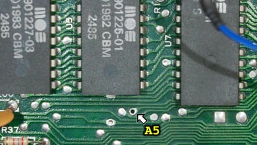
The A5 and A8 address line can be found on the mainboard below the character ROM (U5) and CPU (U7) respectively (on this version of the mainboard - this may vary). See pictures below.


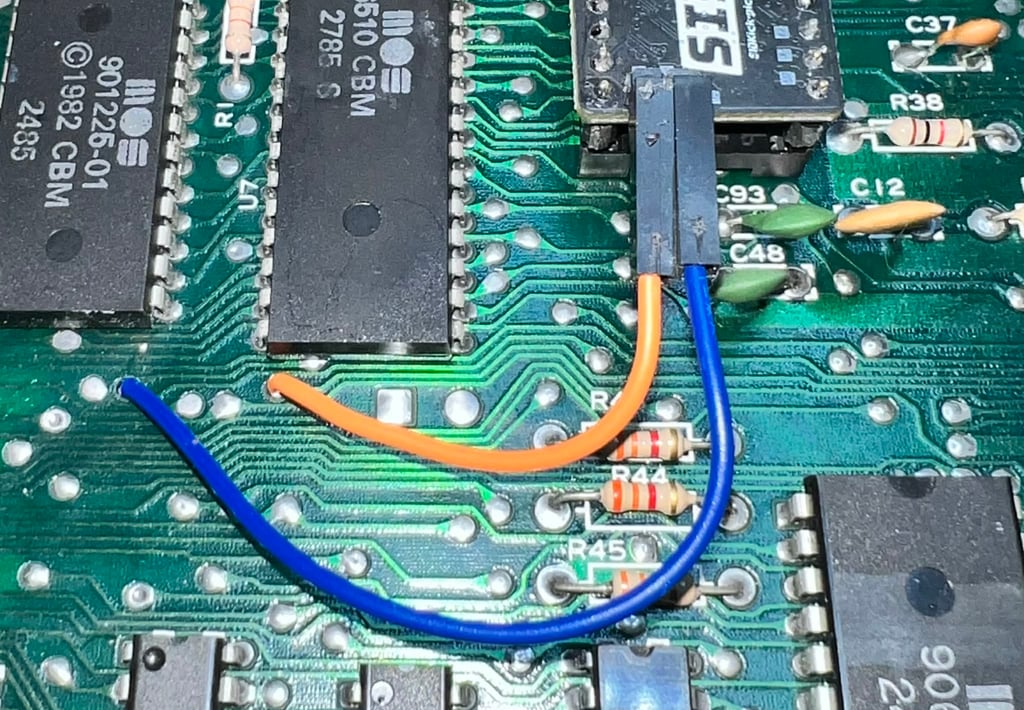
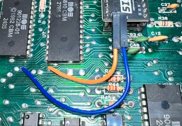
Two Dupont wires are used to connect A5/A8 to the SIDKick Pico where one end is soldered directly to the mainboard, and the other end is attached to the SIDKick Pico with connectors. This will make it easier to perform any maintenance later.
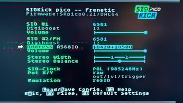
To verify that the connection is working, and correct, the machine is powered on and the SIDKick Pico configuration menu started (SYS 54301). As can be seen from the picture below the SIDKick Pico now detects that address lines A5 and A8 are connected (highlighted in the config menu).

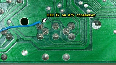
Connecting the DAC output
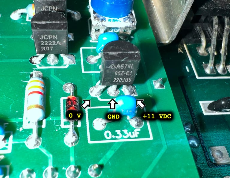
To get the best audio quality the DAC output is connected to:
DAC (LEFT) to PIN #3 on the audio/video connector - this is the normal MONO audio connector on the Commodore 64
DAC (RIGHT) to PIN #7 on the audio/video connector - this pin is normally NOT used, but it CAN be used having a proper stereo A/V cable
DAC (RIGHT) to the "INPUT" pin on the new R/F modulator replacement - and set the R/F modulator switch to "EXTERNAL". This will now give stereo audio on the 3.5 mm TRS audio connector.
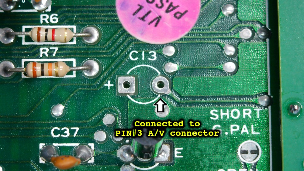
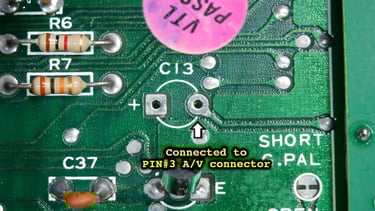
NOTE: It is possible to disable the normal audio output from the SIDKick Pico (the one which is output to the mainboard) by desoldering two jumpers on the SIDKick pico. But I choose not to do so to keep the SIDKick Pico as general-purpose for later use. So to make sure that the "normal" SID audio is not output to the mainboard the capacitor at C13 (10uF / 35V electrolytic) is removed. This will prevent the "normal" SID audio from reaching PIN#3 on the A/V connector. The DAC (LEFT) is then connected to the (now removed) negative side of C13. This point is also connected directly to PIN #3 on the A/V connector. See schematics and pictures below.
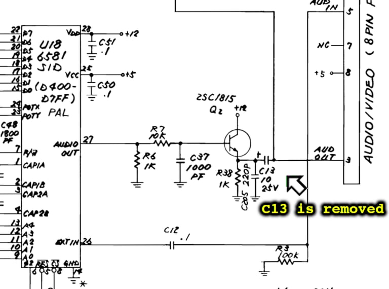
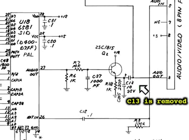
Notice in the schematics above that PIN#7 is marked at "Not connected" (NC) on the A/V connector. So this pin is actually available for a custom made stereo A/V cable (these can be purchased by various sellers). But to connect the DAC (RIGHT) a solder point on the backside of the mainboard is used.

Below is a picture of all the wiring in place. The wires will be fastened with some insulation tape or hot glue later.

During the assembly process the SID Kick Pico 2040 DAC was tested - see video below. As can be seen from the video there is a small multi colour LED on the top of the chip also. This LED is not so visible from the outside, but it is there:-)

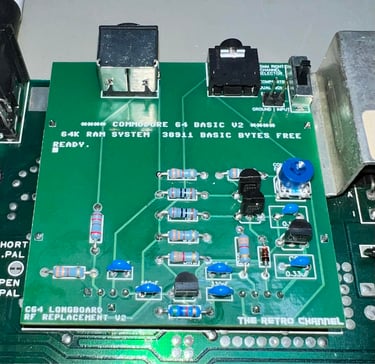
With the SID Kick Pico 2040 DAC in place, and all the supporting cables, the refurbish of the mainboard is complete. NOTE: Due to the size of the SID Kick Pico there are no space for the RF-shield. But this should not be of any problem: the SID Kick Pico does not get very hot and there are heat sinks on the VIC-II. The other ICs should be ok without the RF-shield.
Below are some pictures of the mainboard after refurbish.

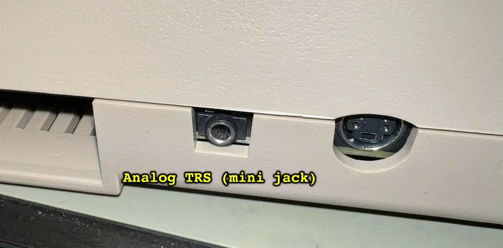
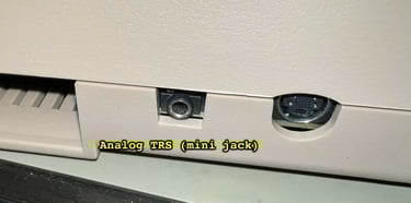
The analog audio from the DAC is output on the TRS (mini jack) connector at the back.
Testing
Proof is in the pudding - does it work?
Testing is done through three main stages:
Testing the basic functionality and chips
Testing the complete set of custom ICs and I/O ports
Testing by using the machine playing demos, games etc. accessed by both floppy and datasette to verify correct operation
NOTE: The image quality is poor. But that is not because of problems with the machine, but caused by a poor video monitor.
Basic functionality and chips
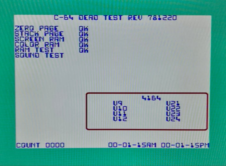
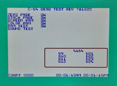
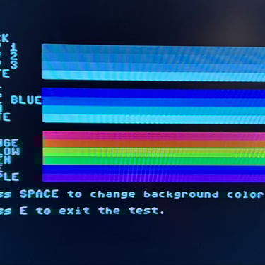
First test is done using the Dead Test Cartridge. This test doesn´t test all the functionality of the Commodore 64, but it does test the basic functionality of the major chips such as the CIA #1/2, CPU, VIC-II, PLA, RAM and SID. As the picture shows below the test is passed.
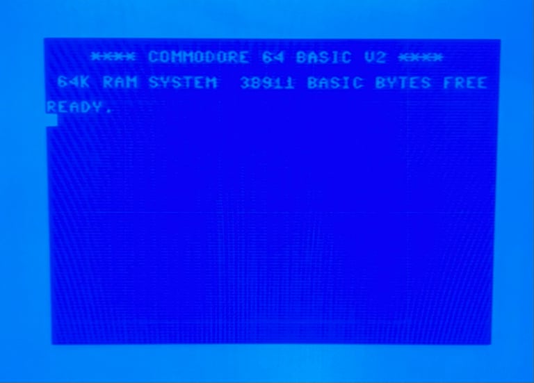
Next test is to power the Commodore 64 to the blue boot up screen and also check the keyboard to make sure all keys works as they should. The test is passed; all keys works and 38911 BASIC Bytes Free.
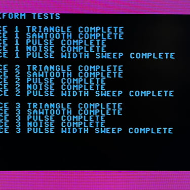
The basic functions of the VIC-II, SID and RAM is tested with 64 Doctor, Commodore 64 SID tester and DesTest cartridges. Note that this is to be considered as basic functionality - more advanced (?) functionality such as sprite handling / collision detection / advanced audio will be tested later.
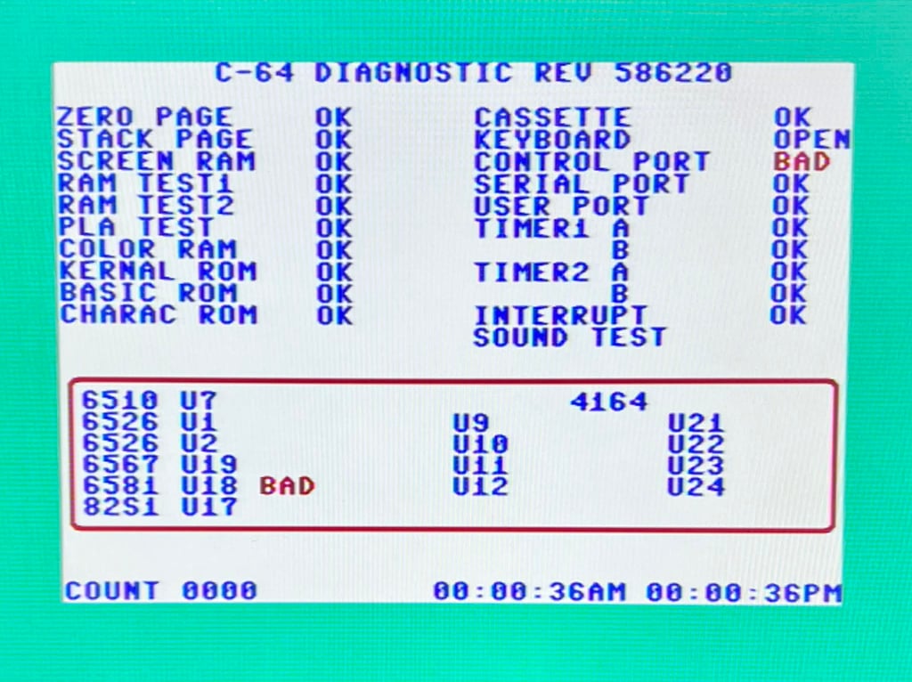
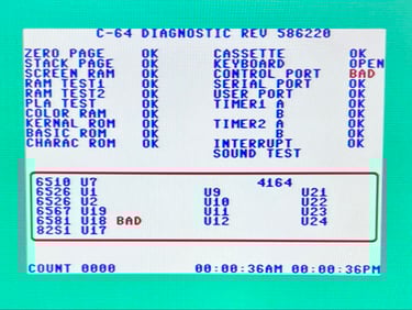
Diagnostics test with harness
To test all the custom ICs, and I/O ports, the Diagnostics cartridge is used. The Diagnostics cartridge is very valuable when the complete test harness i installed as in "everything" is tested formally. As can be seen from the picture below all tests PASS - except from one! The CONTROL PORT says "BAD". But (!) I think this is not correct. The reason why it shows bad is due to the SID Kick PICO 2040 DAC. The test which fails is related to the analog paddle input on the control ports and the 6581 (SID), but these should be just fine. With the SID Kick Pico you can in fact adjust how sensitive these inputs should be in the configuration menu (SYS54301). So even if it says "BAD" this should be just fine. The control ports works just fine.
Extended testing
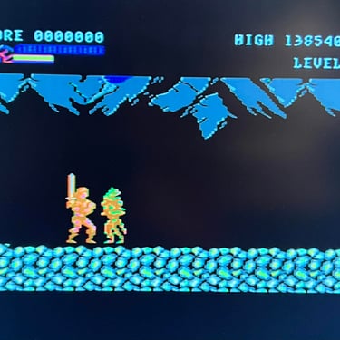
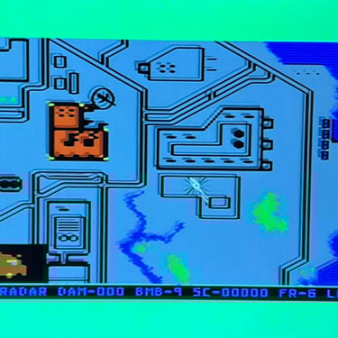
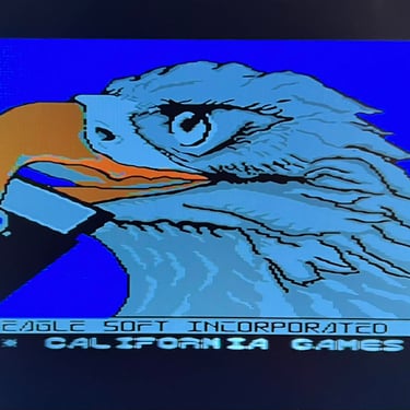
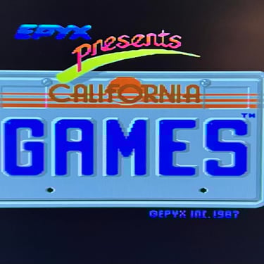
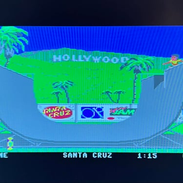
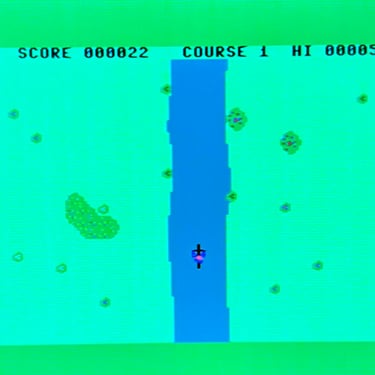
Knowing that the basic functionality of the machine works I continue the testing by using the Commodore 64 for normal operations; playing some games, watching demos, loading from datasette and floppy and using a cartridge. I can not find any issues with this machine. I also pay special attention to the video to make sure that there are no glitches in the graphics - I can´t see any abnormalities. Below is a gallery with pictures from the testing. NOTE: The colours on the pictures are completely off and the image quality is poor. But this only due to my poor TV and not due to the machine.


Final result
"A picture worth a thousand words"
Below is a collection of the final result from the refurbishment of this C64. Hope you like it! Click to enlarge!


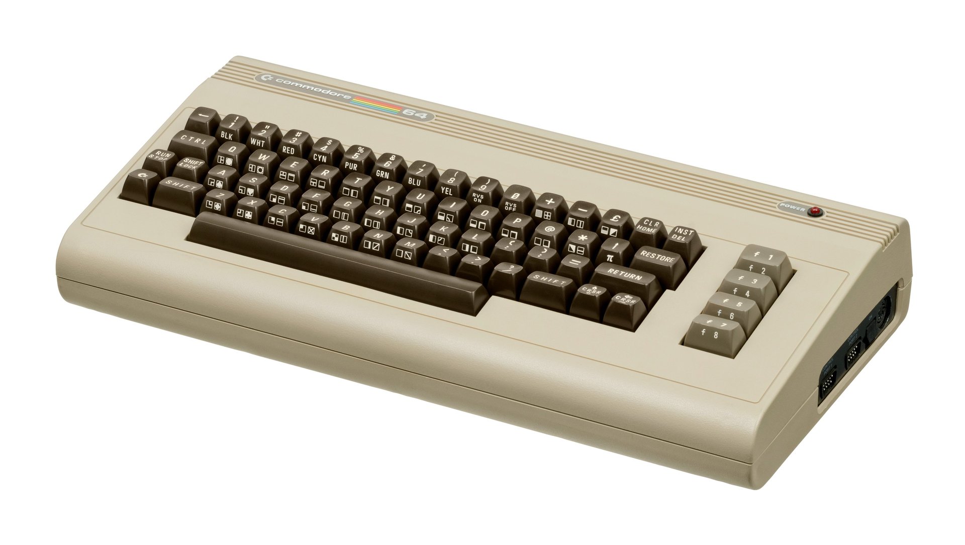
Banner picture credits: Evan-Amos