
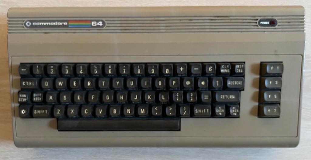
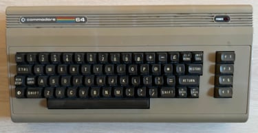
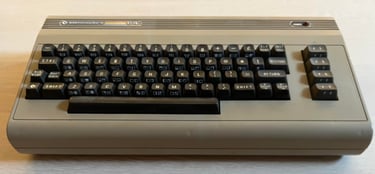
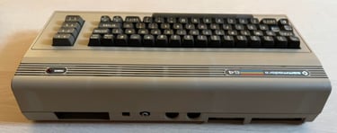
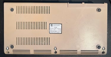
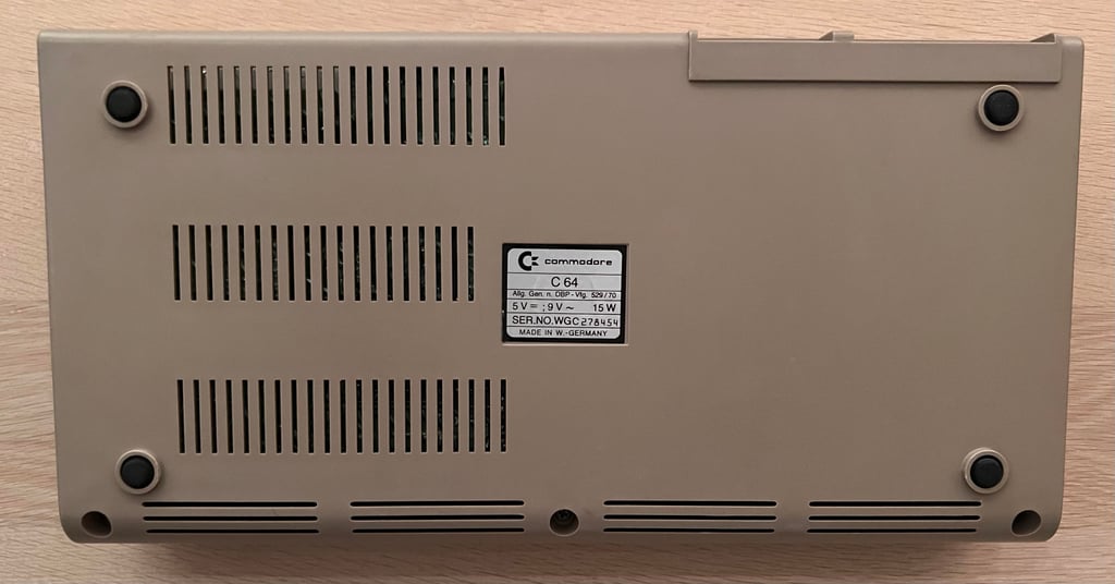
C64 Breadbin
Ser. No. 278454
Assy 250425
P/N 251470-01 (REV A)
Starting point
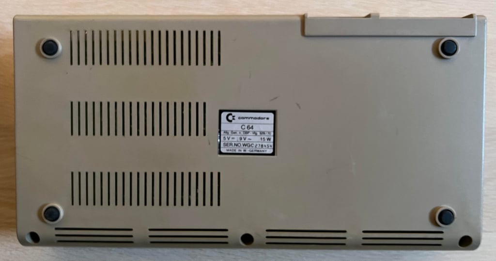
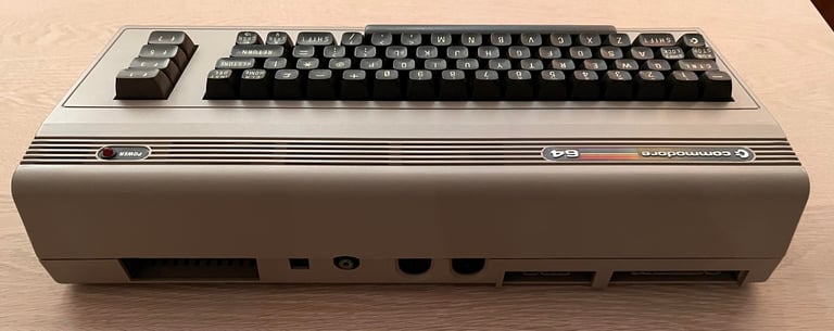
This C64 breadbin has come to me for some repair and refurbish. The machine is known to be non-working - I don´t yet know what the symptoms are. From the outside the machine is quite dirty and with some discolouring. But on the positive side it looks to be mostly undamaged. I can not see any severe issues from the outside, but I notice the following:
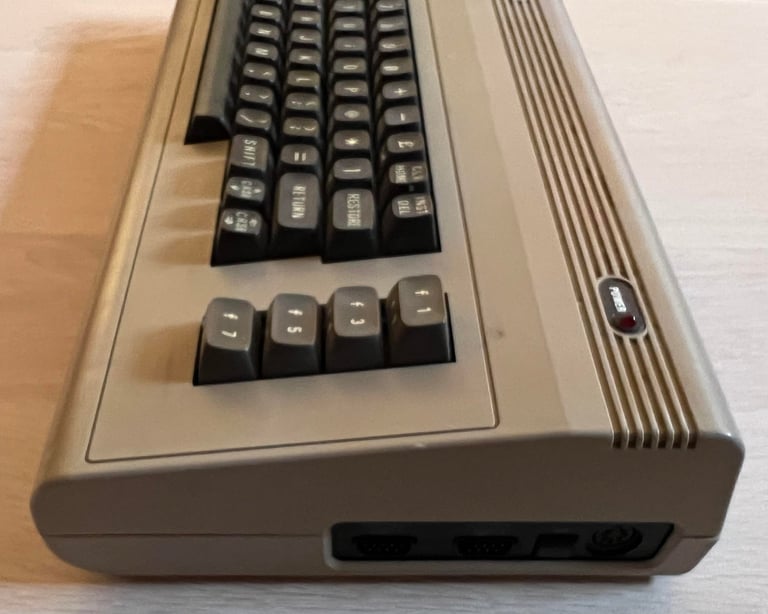
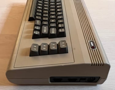
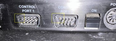
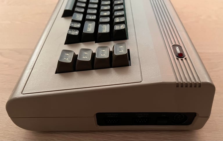
In the PORT # 2 joystick connector one of the pins are missing (or pushed in). And there are some cracks in the port housings.
There are some small dents from the screws in the bottom part of the casing protruding into the top casing.
Below are some pictures of the machine before refurbishment (notice that the quality of these images are low unfortunately).


Refurbishment plan
The refurbishment plan for this C64 breadbin (several of them in parallell):
- Clean and remove stains from the casing
- Clean and restore the keyboard
- Refurbish main board (cleaning, checking, repairing, replacing capacitors and voltage regulators, adding heat sinks etc.)
- Recap RF-modulator
- Verify operation by testing
The plan can be updated during the refurbishment process. Sometimes I discover areas that needs special attention.
Opens it up...
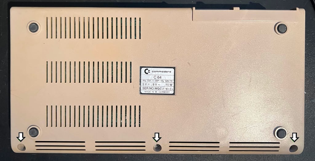
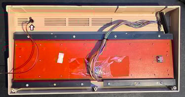
To start to open the Commodore 64 the three screws at the bottom are removed (indicated by the arrows).
The top cover is tilted about 30 degrees and then carefully wiggled until the rear clips releases. Then the top cover is tilted to 90 degrees. As can be seen from the picture below the inside looks to be intact - but it is quite dirty which is normal after almost 40 years. Two of the screws holding the PCB are missing (see arrows). I would assume that someone has been here before.
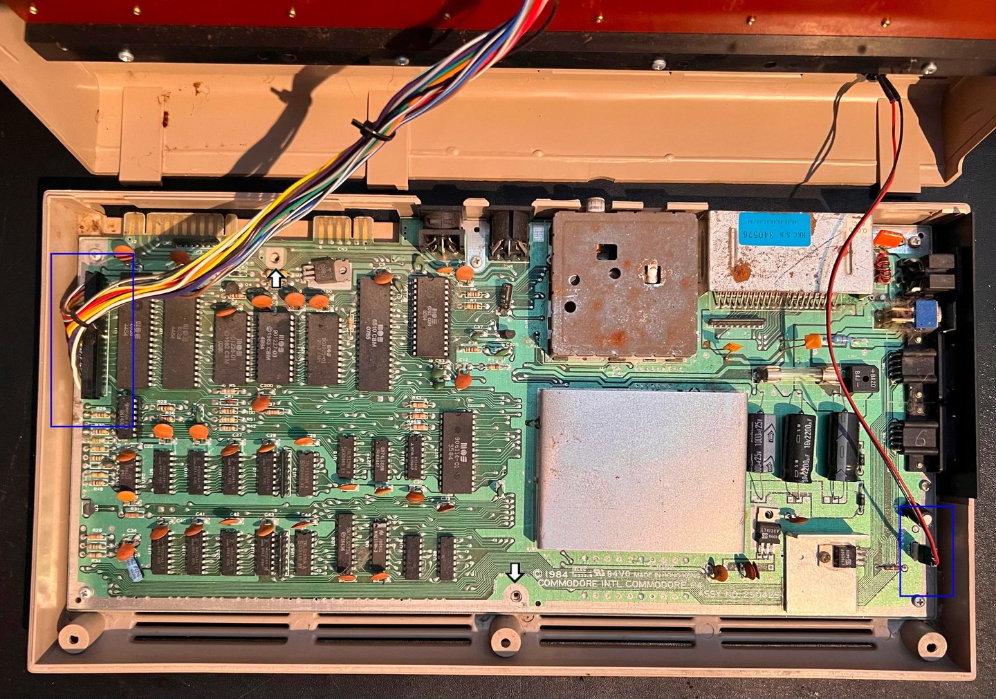
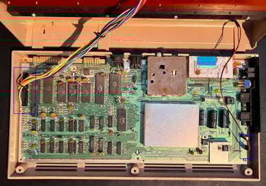
Keyboard- and LED connectors are removed (see blue squares). The remaining screws holding the PCB to the bottom cover are removed. Note that there are also two small machine screws holding the metal port bracket (see arrows in the picture below). These are removed and kept separately.
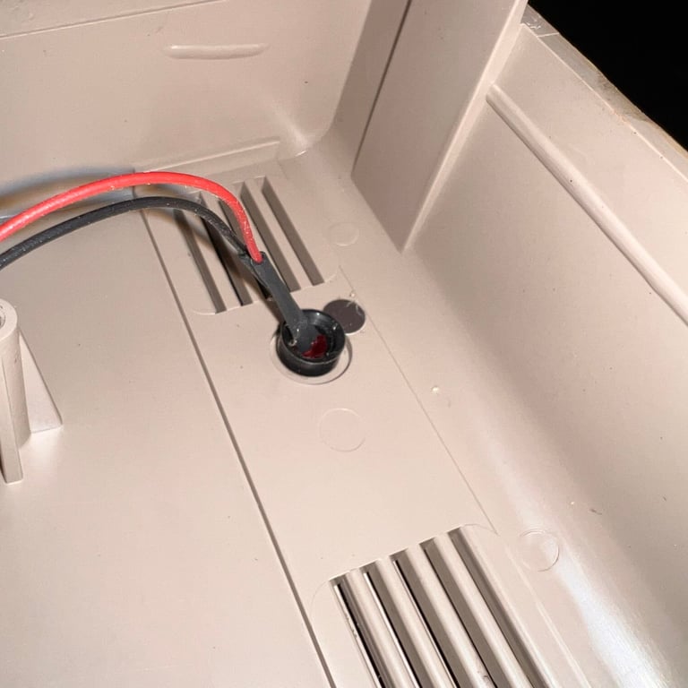
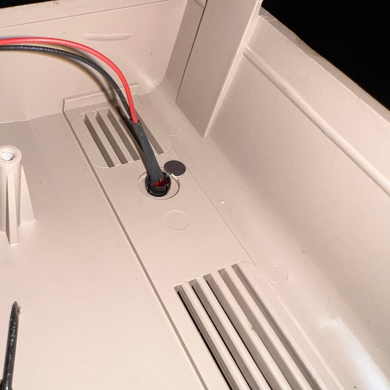
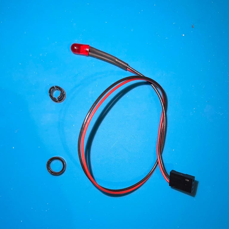
Although not strictly necessary I find it good practice to remove the LED from the top cover (see arrow below). Also the eight screws holding the keyboard to the top cover are removed.

Removing the LED is quite straightforward, but it can be good to know how to do it. First, remove the small circular ring from the LED clip. Then push the LED itself from the outside of the cover towards the inside - it will "pop" out of the small clip. Finally, push the small plastic clip from the inside of the cover towards the outside. See pictures below.
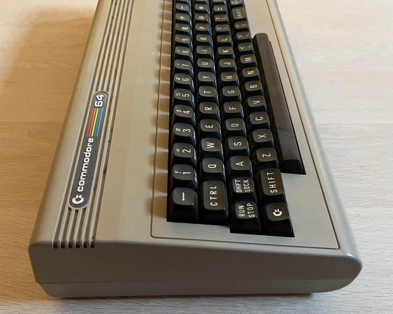
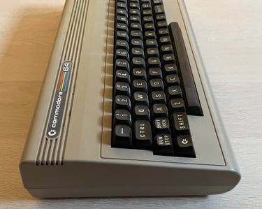
Exterior casing
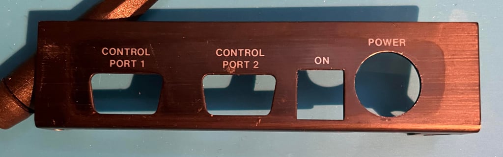
The top- and bottom cover needs thorough cleaning. But before the top cover is cleaned the two badges are removed. To remove these some hot air from a hair dryer is applied to the badges and with a small scalpel the badges are pried off. Interesting, the "POWER" badge is just a sticker - not the traditionally metal badge.
Both top- and bottom cover are cleaned thoroughly with mild soap water. This removes most of the dirt. The toughest stains are removed with isopropanol.
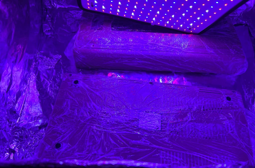
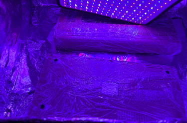
After cleaning the covers are retrobrighted. This is done by applying hydroperoxide cream (12 %) frequently while placing the covers in UV-light.
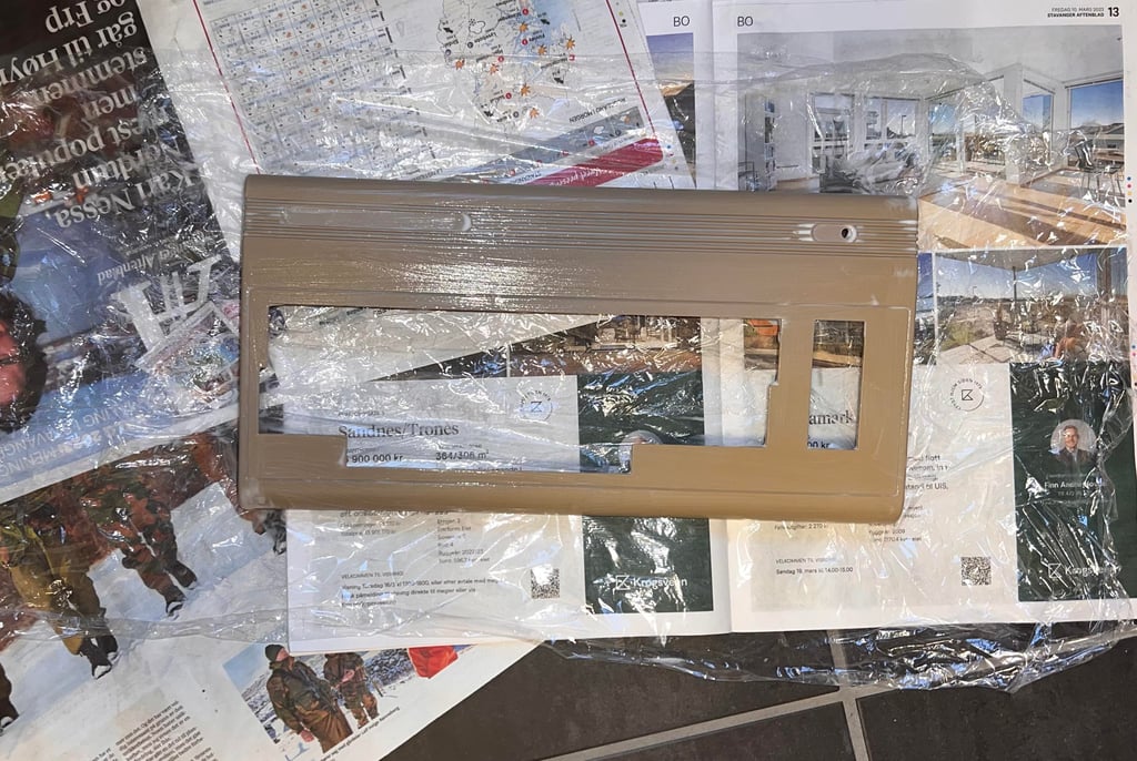

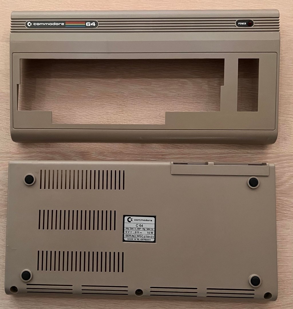
The result after retrobrighting is quite good I think. Most of the discoloration is gone and the most of the original grey color is back. Below is a picture of the top- and bottom cover after retrobright.

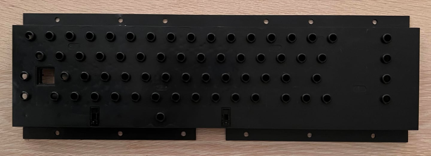
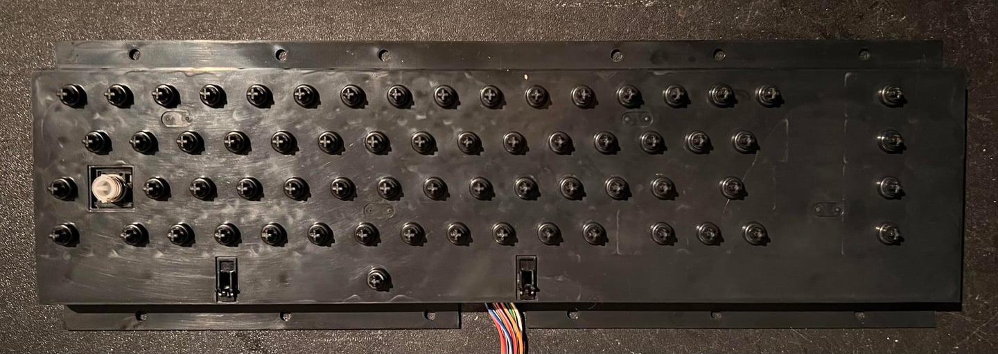
Keyboard
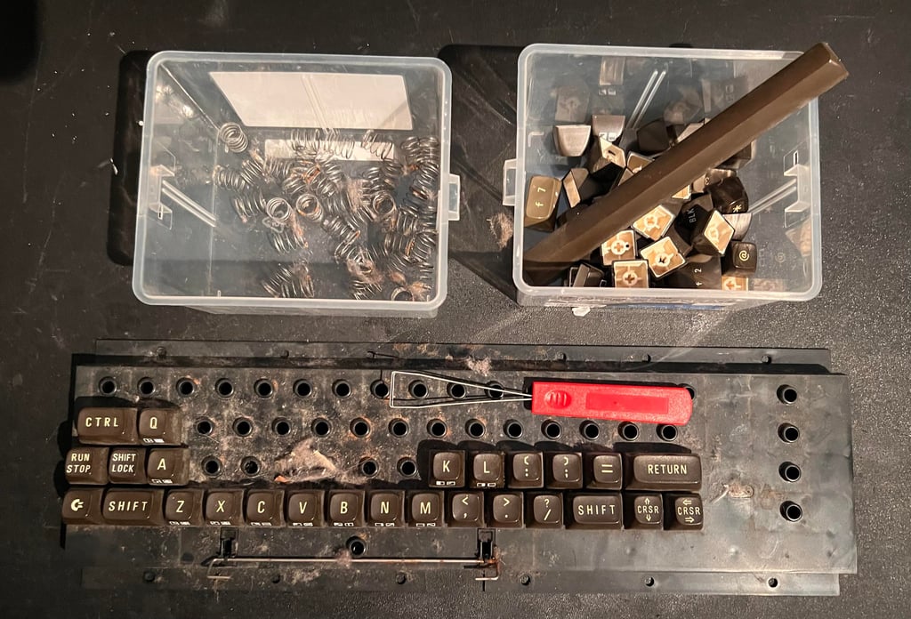
The keyboard needs to be properly refurbished. All the small machine screws are removed from the backside of the keyboard - but before that the two wires are desoldered from the SHIFT LOCK. See picture gallery below.


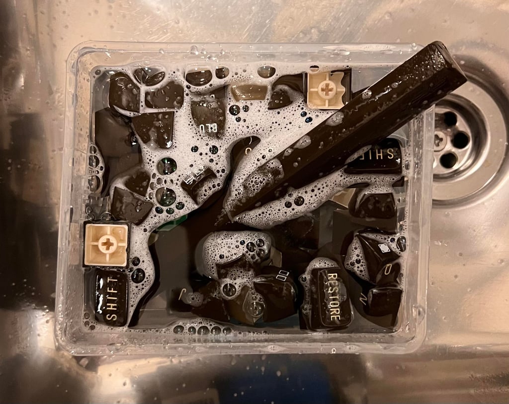
All the keys are removed to that both keycaps and plastic casing can be cleaned. To remove the keycaps a special keycap puller is used - this will reduce the risk that both key and plunger are damaged. As can be seen below the keyboard is quite dirty - so a good clean is very welcome. Note that the spring beneath the spacebar is a bit bigger than the rest of the springs. So it is good practice to keep this spring in a separate bag.

The keycaps are placed in a box of soap water and some glass cleaning spray for about 12 hours to remove most of the grease.

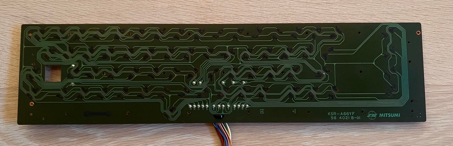
For the keyboard plungers to make good contact the keyboard PCB is cleaned carefully with some isopropanol. This is a MITSTUMI KSR-A66YF keyboard PCB where the contacts are made of small carbon pads. Below is a picture of the keyboard PCB after cleaning.
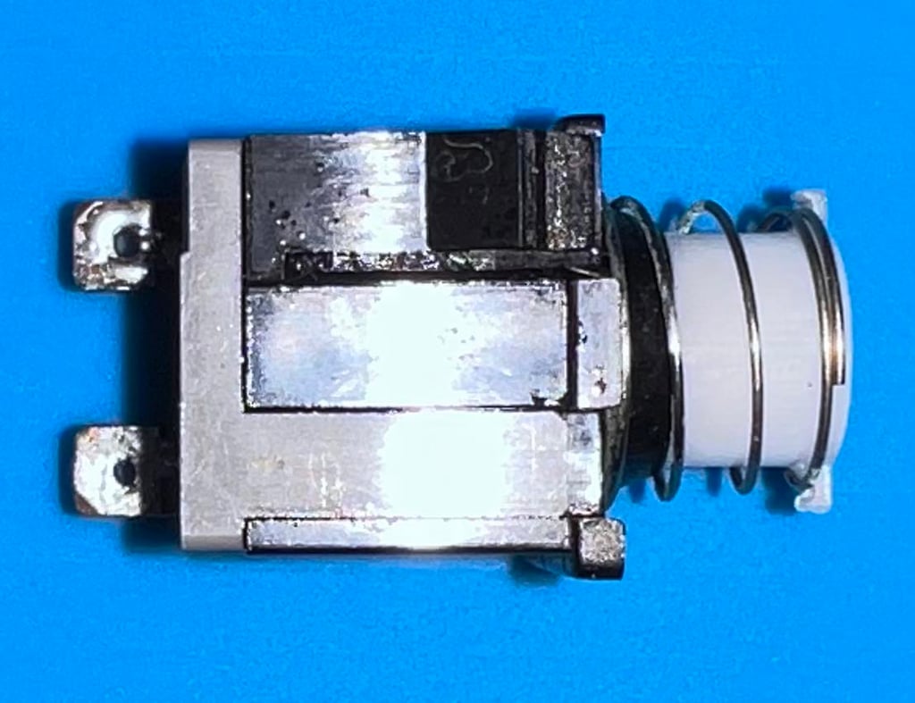
The SHIFT LOCK key mechanism looks be in good condition (HINT: to get the SHIFT-LOCK key out of the keyboard push firmly from the back towards the front of the keyboard casing). There is a good "clicking" sound and the key can be set in both position. The key is cleaned with some contact cleaner. See picture after cleaning.

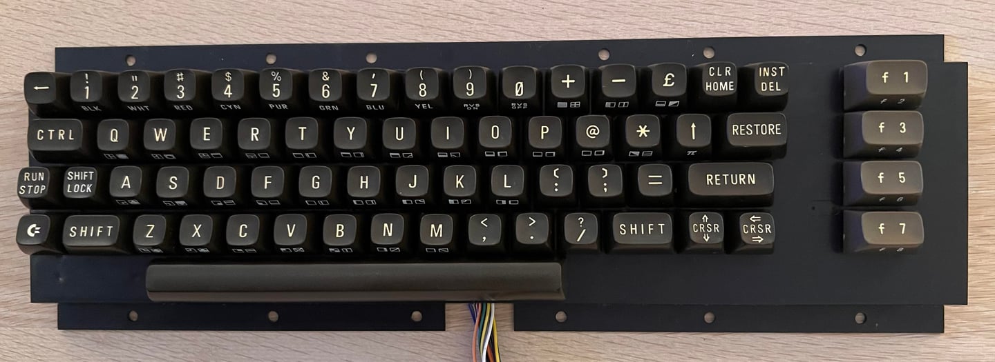
After cleaning the keyboard plastic housing looks very nice. Almost like new (!).
All plungers are carefully cleaned with isopropanol. I do not always clean the plungers with isopropanol, but the plungers were quite dirty so I think this is the right decision.
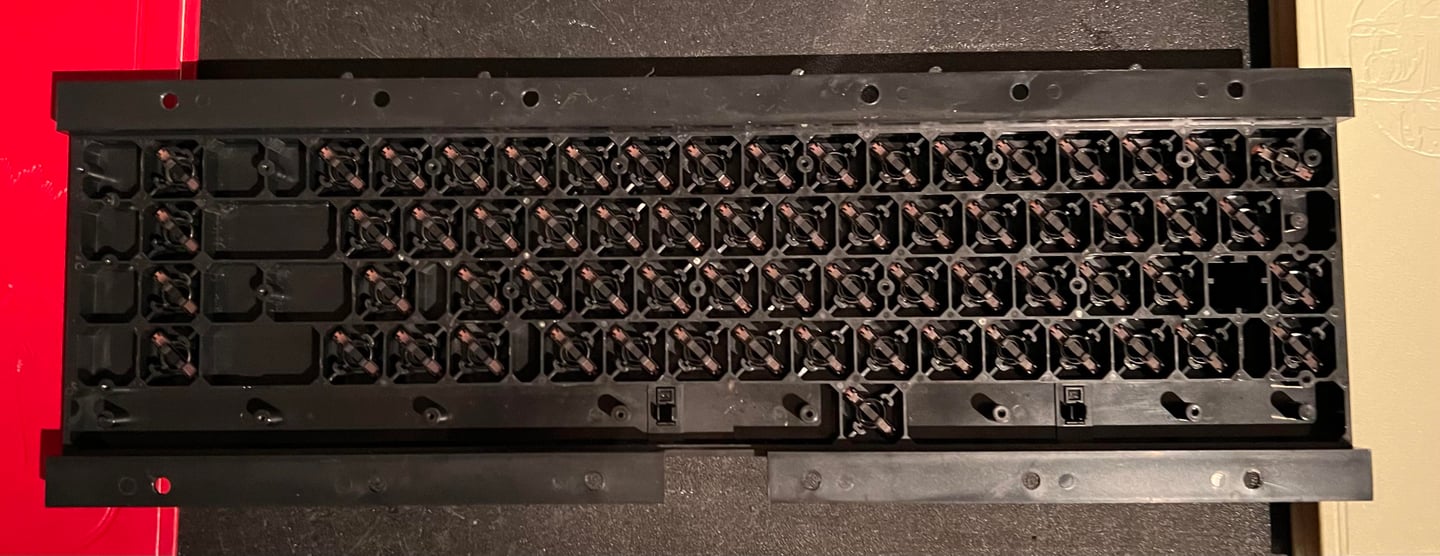
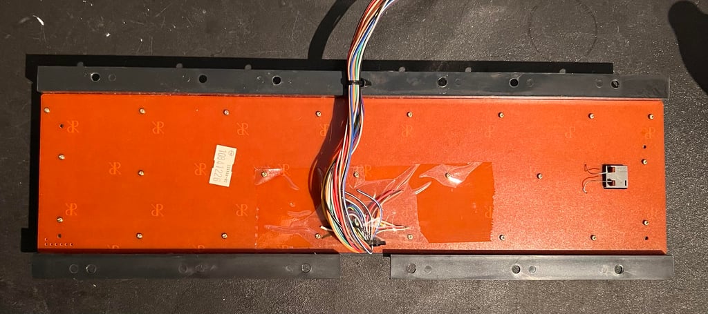
The PCB is reattached and all the keys are put back on the plungers. The result is very good I think.
Mainboard
Preparations
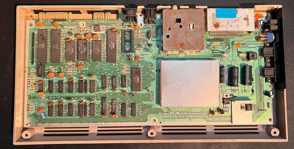
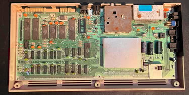
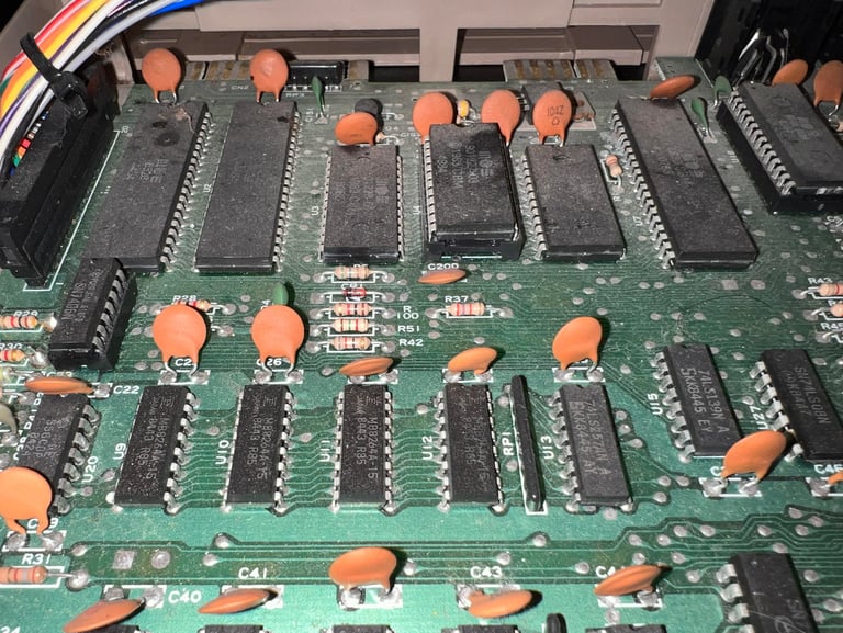
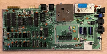
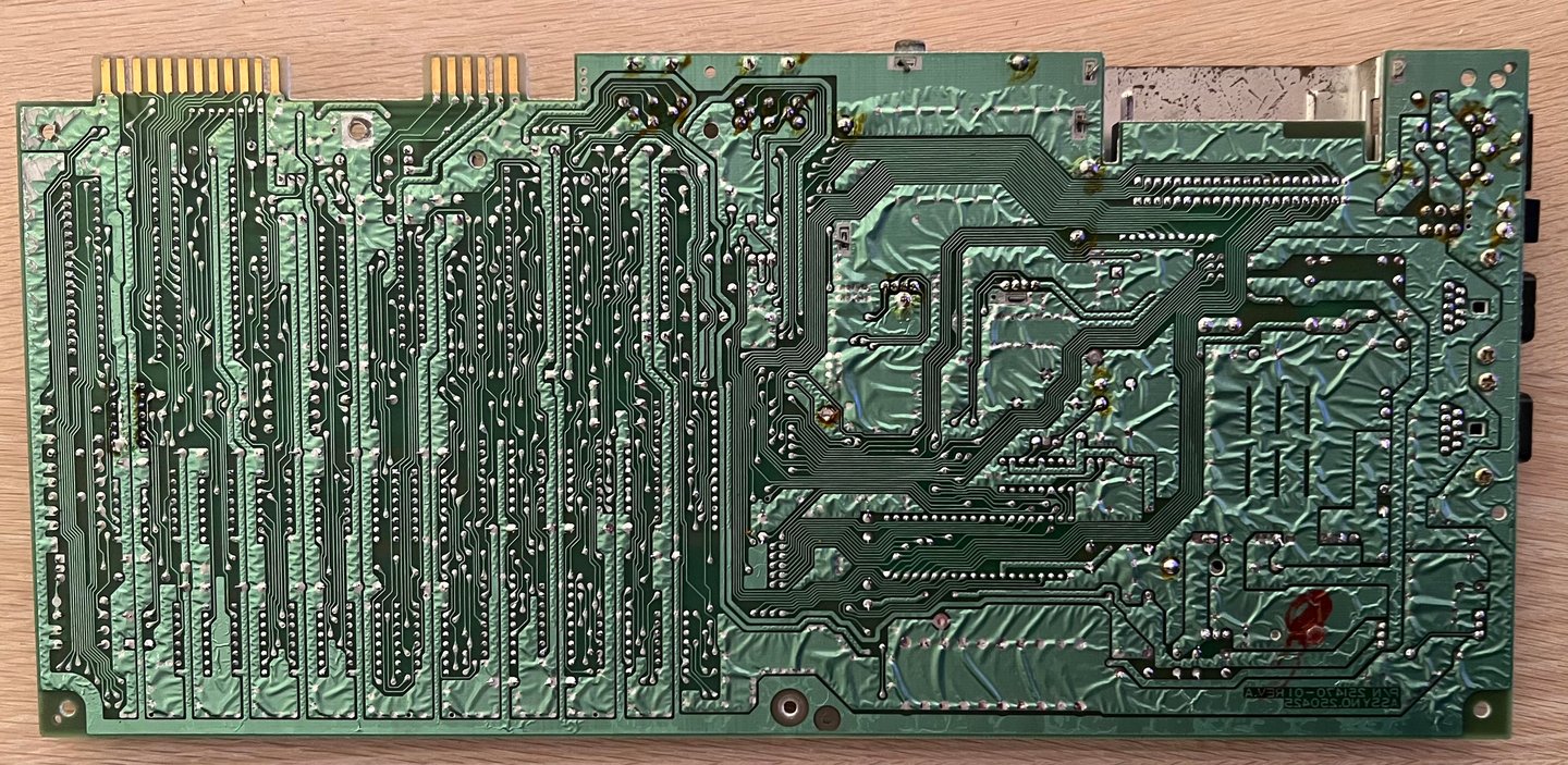
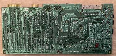
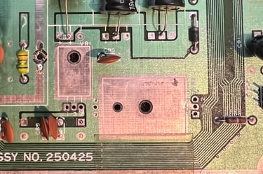
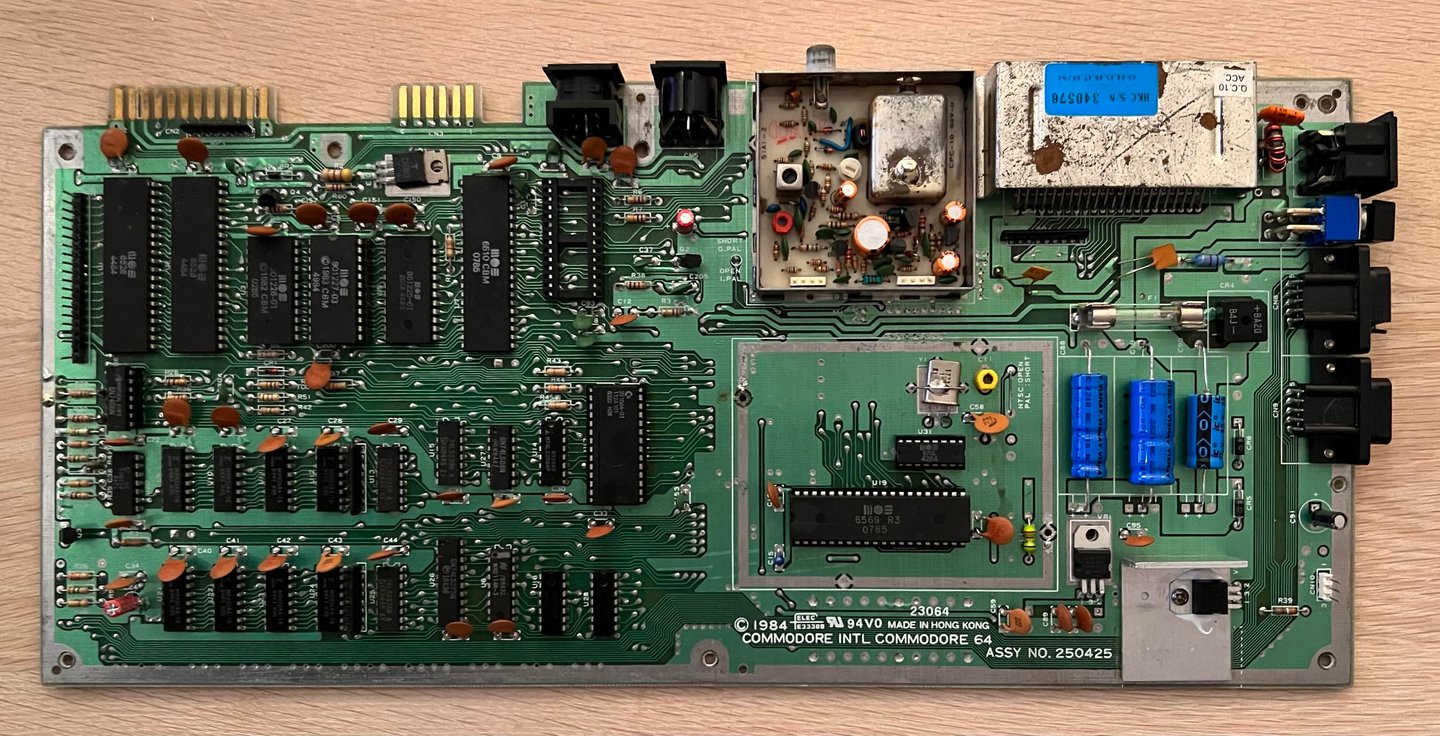
This mainboard revision is assy 250425 P/N 251417-01 Rev A - and it supposed to be not working. As mentioned the mainboard is quite dirty (which is normal) so before I start the repair and refurbishment the mainboard needs to be cleaned. Below are some pictures of the mainboard before cleaning.
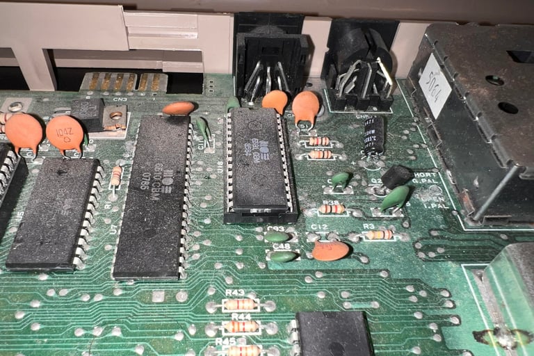
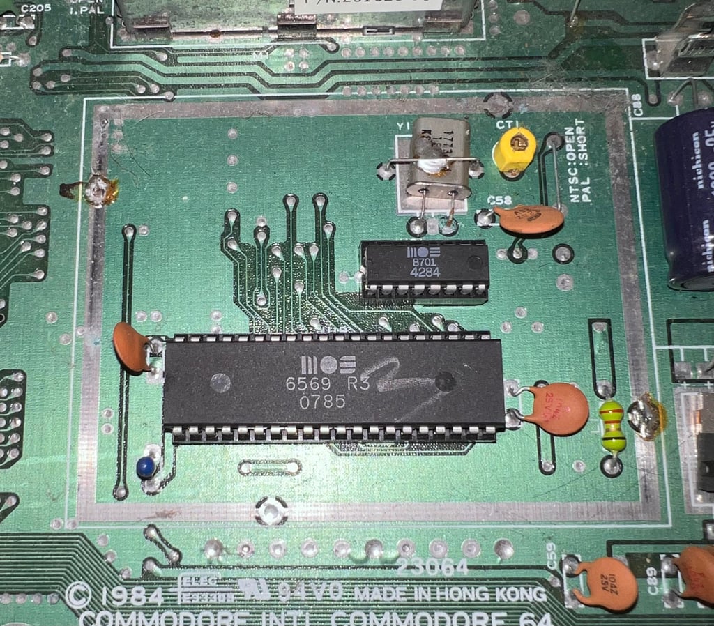
Also before cleaning the RF-shield surrounding the MOS 6569 VIC-II chip is desoldered and removed. This RF-shield has no purpose in modern times - it only encapsulates heat which can deteriorate the VIC-II chip. Below is a picture of the VIC-II after the RF-shield is desoldered.

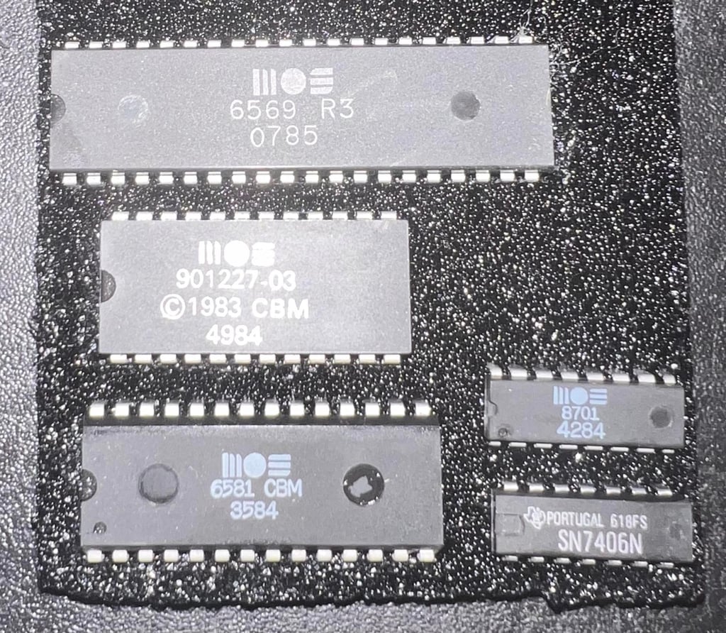
Some of the chips are socketed and removed before cleaning the mainboard (also the fuse is removed):
MOS 6569 VIC-II
MOS 6581 SID
MOS 901227-03 KERNAL
MOS 8701 Clock circuit
SN7406 Hex inverter buffer
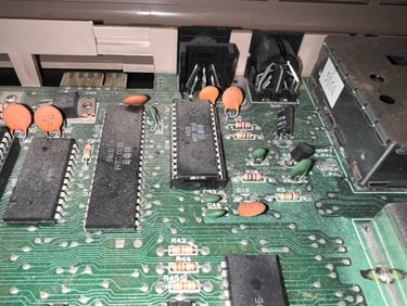
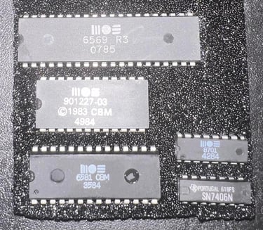
All of the chips are refurbished by brushing all the pins with a glass fibre pen and cleaned with isopropanol. See picture below of the ICs after cleaning.
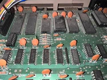
The mainboard is cleaned properly with mild soap water and a paint brush. After cleaning the PCB is left to dry for about 24 hours - and periodically sprayed with isopropanol to speed up the evaporation. The mainboard looks very good after cleaning. See picture below.

Visual inspection
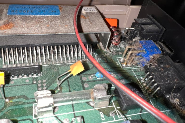
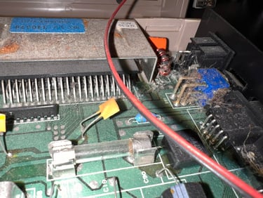
This mainboard looks to be without any damage as far as I can see. There are no sign of corrosion, ripped traces or bodge wires. What I note:
There is sign of some rework; the SN7406 (Hex inverter) is both socketed and as can be seen from the picture below there are signs of flux residue.
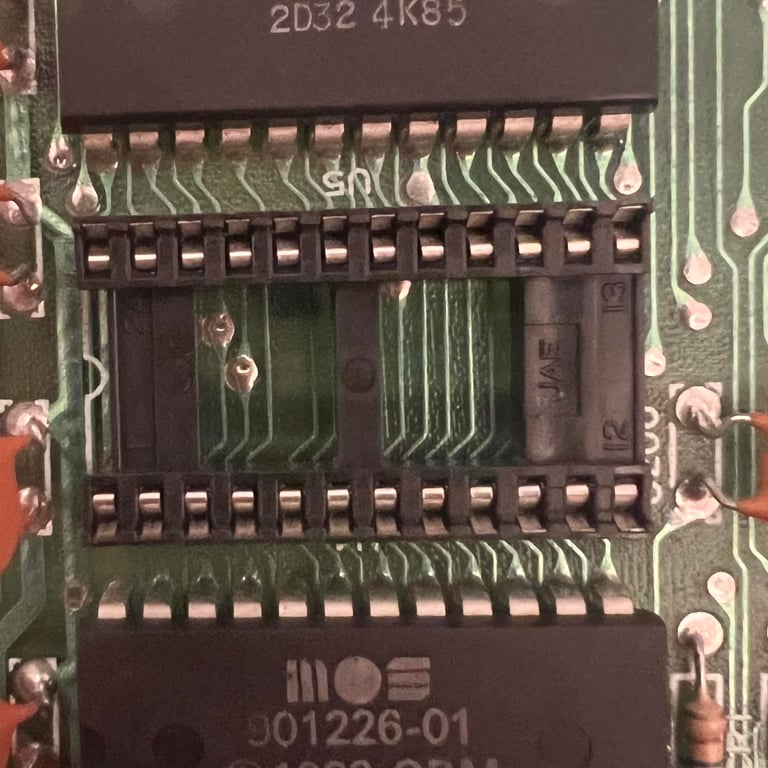
All of the sockets are single-wipe except for the KERNAL (U4). Could it be that this has been replaced? There are no sign of flux residue.
There are some minor signs of oxidation in the SID (U18) and VIC-II socket (U19). This will be cleaned with isopropanol later.
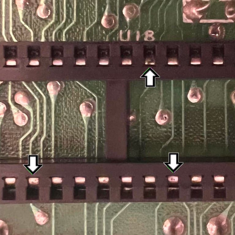
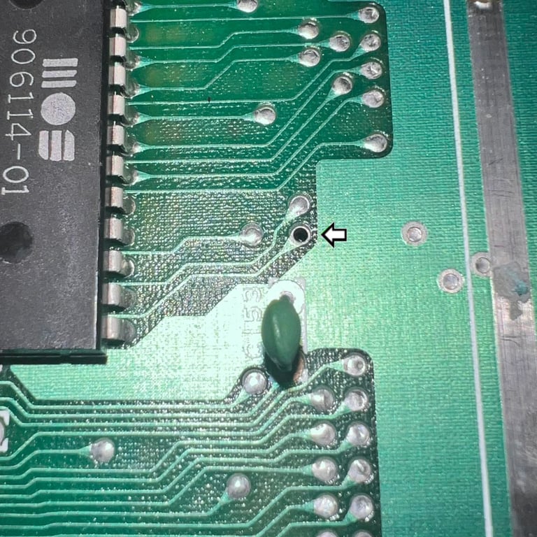
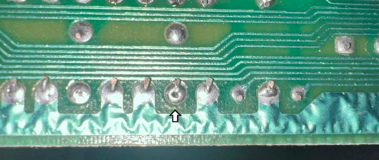
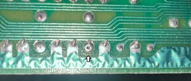
Two of the vias on the PCB are not soldered. Why? If I compare with a mainboard of same revision they should be soldered.
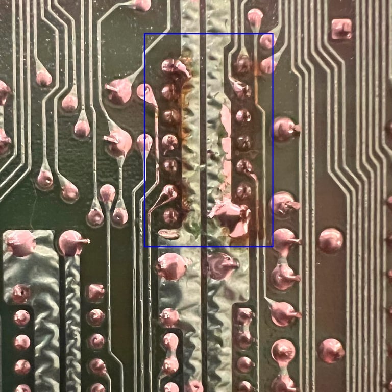
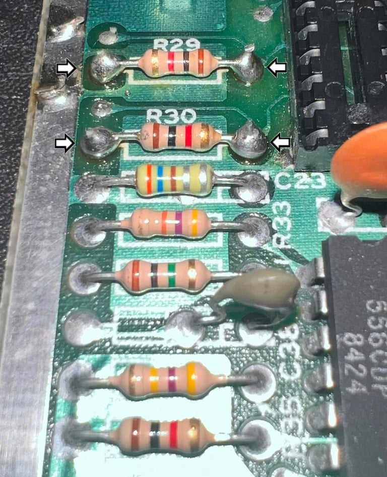
R29 and R30 are poorly soldered. There are large blobs on the top side of the PCB and at the bottom it is possible to see that the soldering is not complete.
Below are some pictures from the above mentioned comments.
In the table below the main chips are listed (before refurbishment - some may be changed during repair if required).

Intial testing
The machine is supposed to be non-working, but before I turn on the power I check for short circuit at the +5 VDC and 9 VAC rail (at the user port) with a multimeter. The position of these can be found in my Checking C64 voltages article. A short circuit here could cause damage to the power supply. Luckily, no short circuit is detected so the machine should be safe to power on. Before powering on the power connector and the on/off switch are sprayed with electro cleaner and "massaged" (read: the power cable is inserted/retracted multiple times, and the power switch turned on/off many times.
Result with power on:
Black screen - but there seems to be a video signal
None of the chips get abnormally hot
This is a quite common symptom. The "black screen" can be caused by several problems.
Checking the voltages
Voltages are measured before - and after - refurbishment. This is to make sure that all voltages are within acceptable levels. This table is updated after refurbishment is completed. All voltages are measured according to the article Checking C64 voltages. As seen in the table below all voltages are within acceptable levels. So there are no obvious reason why the machine is failing to start.
Dead test cartridge
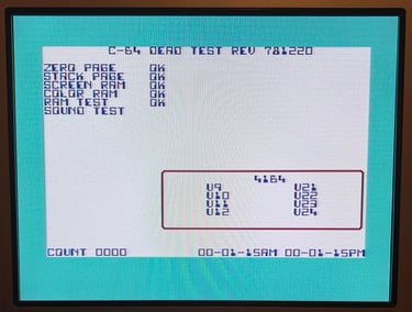
When having a "BLACK SCREEN" the dead test cartridge can be useful. As long as the CPU, PLA and VIC-II are working the cartridge can boot (in theory). Of course, if some of the glue logic are broken this isn´t always the case. So fingers crossed that the dead test will give some information. But, alas, no luck: still a completely black screen - the video signal seems to be there though.
Since the dead test cartridge is not starting at all this lead me to think that the PLA or CPU could be bad.
Checking the CPU signals
With the oscilloscope the major signals are checked. The signals are checked against the CPU signal reference. See table below for results.
As can be seen from the table above the machine is "stuck" not doing anything. The clock, address- and datalines are working hard but nothing happens... this makes me think that the PLA can be bad. The PLA is playing the role as the conductor in the Commodore 64, and if this is broken nothing gets done.
Replacing the PLA
The PLA (U17) is desoldered. No traces or pads were lifted. A new 28 pin dual wipe socket is installed. The PLA is tested in a known working machine and it turns out that the PLA is broken. No surprise there - these are notorious for failing.
A "new" PLA is chip is installed in the machine and powered on. Result: BLACK SCREEN (!) and NO VIDEO SIGNAL out.
What happened now? It might be that there are more than one fault in the machine, but loosing the video signal - I did not see that coming!
Checking the voltages - REVISITED
This is very bizarre... I now see that the 7805 and 7812 voltage regulators are generating the right voltages. But, it takes up to 10 (!) seconds before the voltage ramps up from 0 V to 5 VDC and 12 VDC respectively. Since the +5 VDC from 7805 is used to supply the 6569 MOS VIC-II chip this is the reason why the video signal is missing up to 10-15 seconds.
So there is obviously something wrong with the power. In the schematics below the power circuitry is shown.
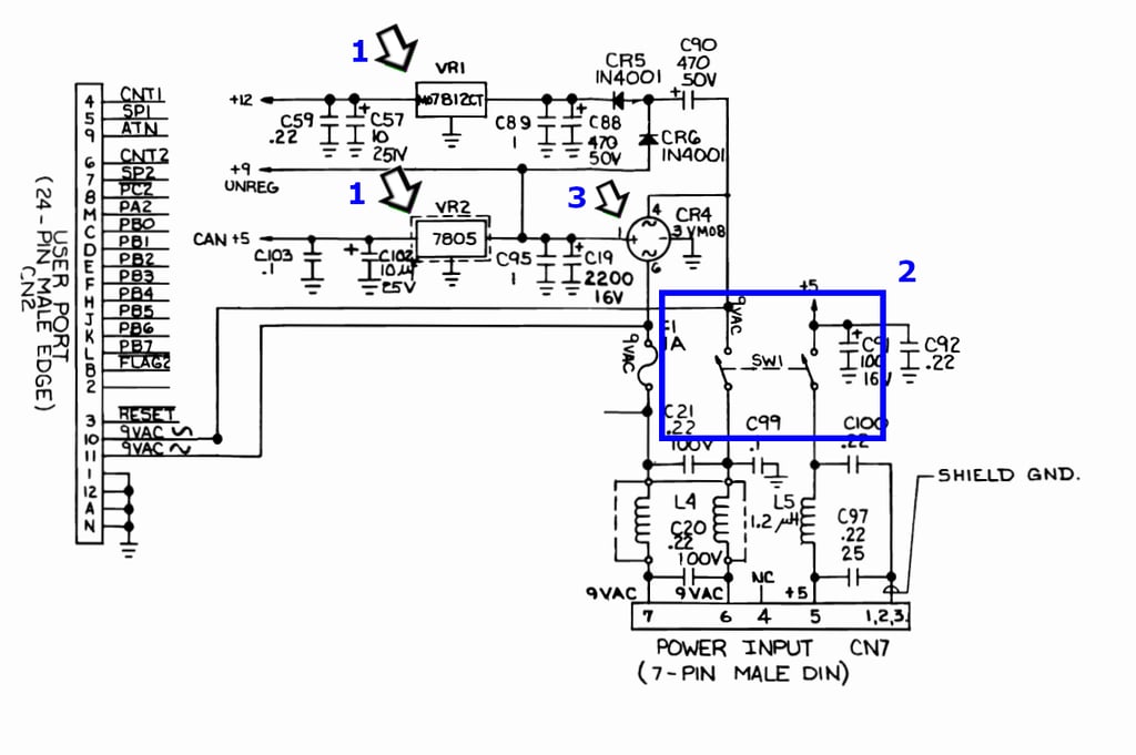
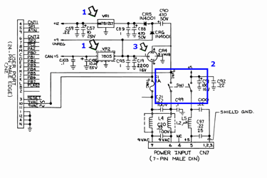
The schematics above also includes the numbers 1-3. These numbers refers to my plan to locate the fault:
Replace the 7805 and 7812 voltage regulators
Check and clean the power switch
Replace the bridge rectifier
At the moment I don´t suspect the C88 (470 uF) or C19 (2200 uF) electrolytic capacitors yet. If they were faulty I would expect that the charging time to be impacted, but not as much as 10 - 15 seconds.
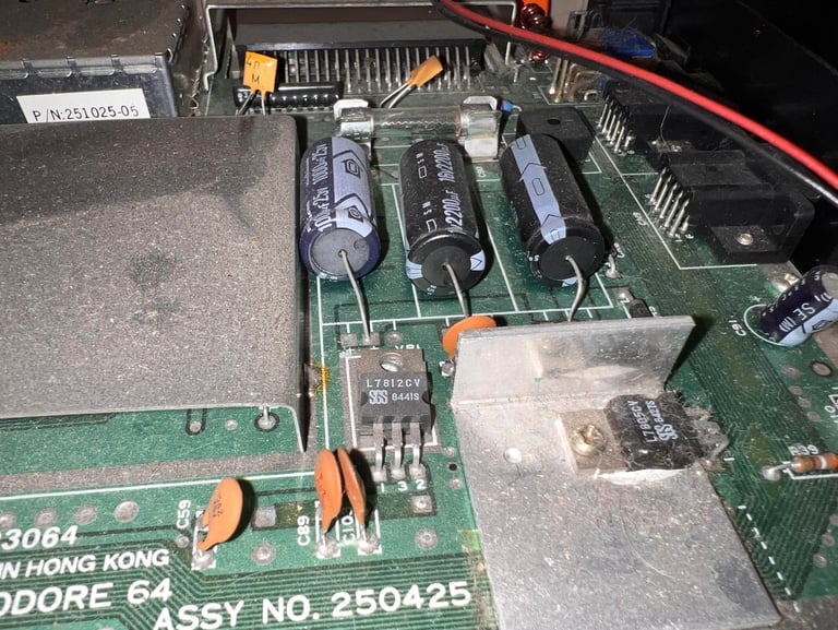
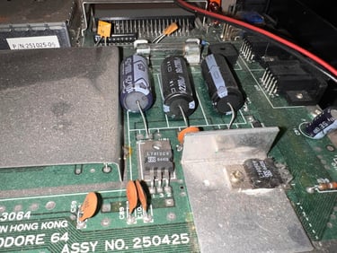
#1 - Replacing the voltage regulators
I don´t really think the voltage regulators are the cause of the fault since both fail to generate the right output. But since these are to be replaced anyhow in the refurbishment I choose to start with these. Please note that one of the pads at the bottom side of the PCB were lost during desoldering. This does not affect the mainboard as this pad was not used to anything (I forgot to take a picture unfortunately). No pads on the front were damaged - but I need to solder on the top side on the 7812 output pin.

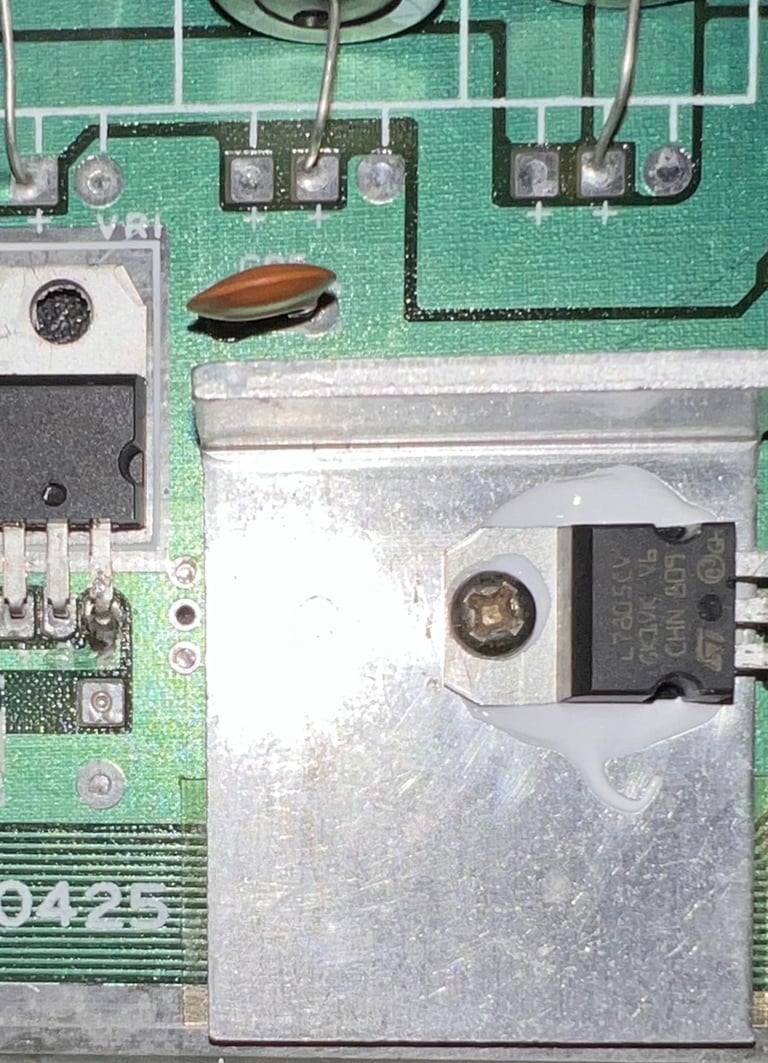
Result is no change unfortunately. I still takes up to 10-15 seconds for the voltages to ramp up to +5 VDC and +12 VDC - and still black screen.
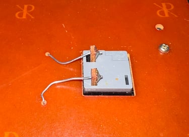
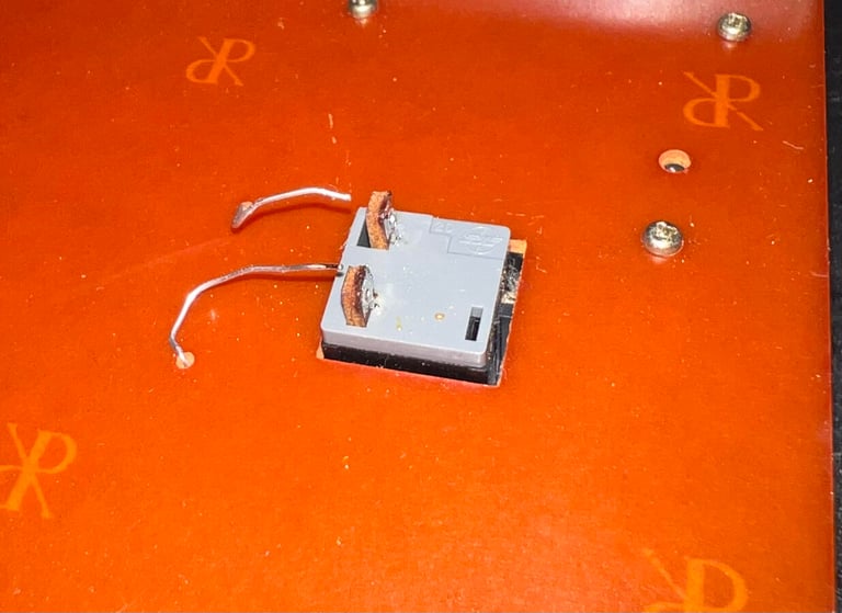
#2 - Check and clean the power switch
As the schematics above shows the power switch connects the +5 VDC and 9 VAC from the power supply to the mainboard. The +5VDC is present at the user port so this is fine, but the 9 VAC is used to create the + 5VDC (for the VIC-II) and the + 12 VDC. And as seen in the beginning of the "Mainboard" chapter the power switch was very dirty.
The power switch is desoldered using both a soldering iron and a desoldering gun. No traces or pads lifted.
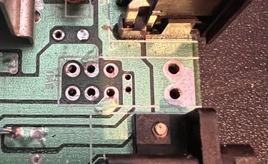

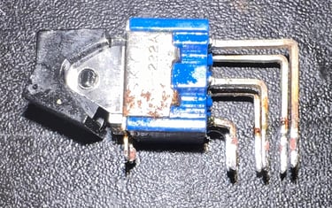
The switch is completely disassembled. And holy moly it is dirty inside. The metal parts are completely covered with grease and dirt. See pictures below.
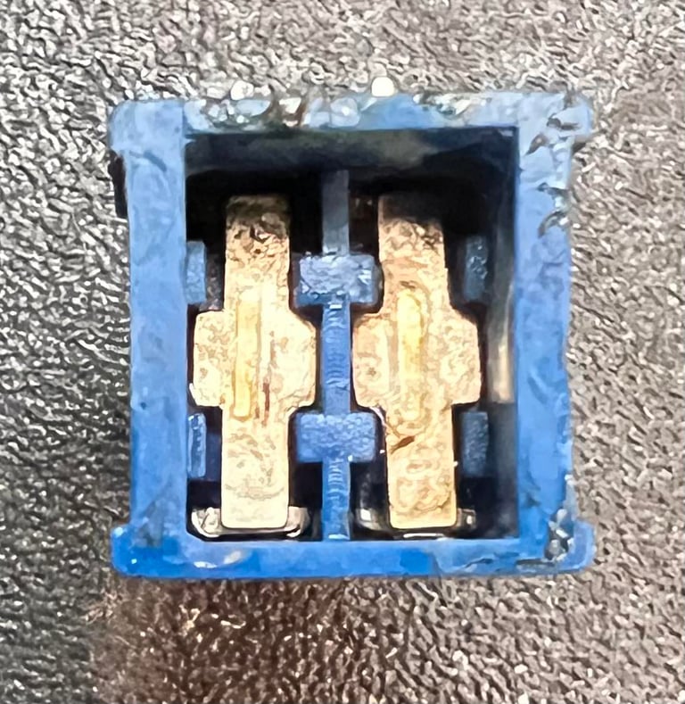
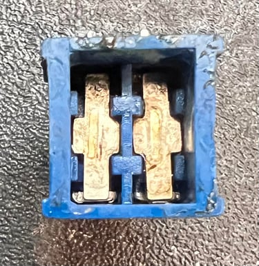
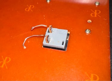
Everything is cleaned carefully with isopropanol while holding the parts with precision tweezers.

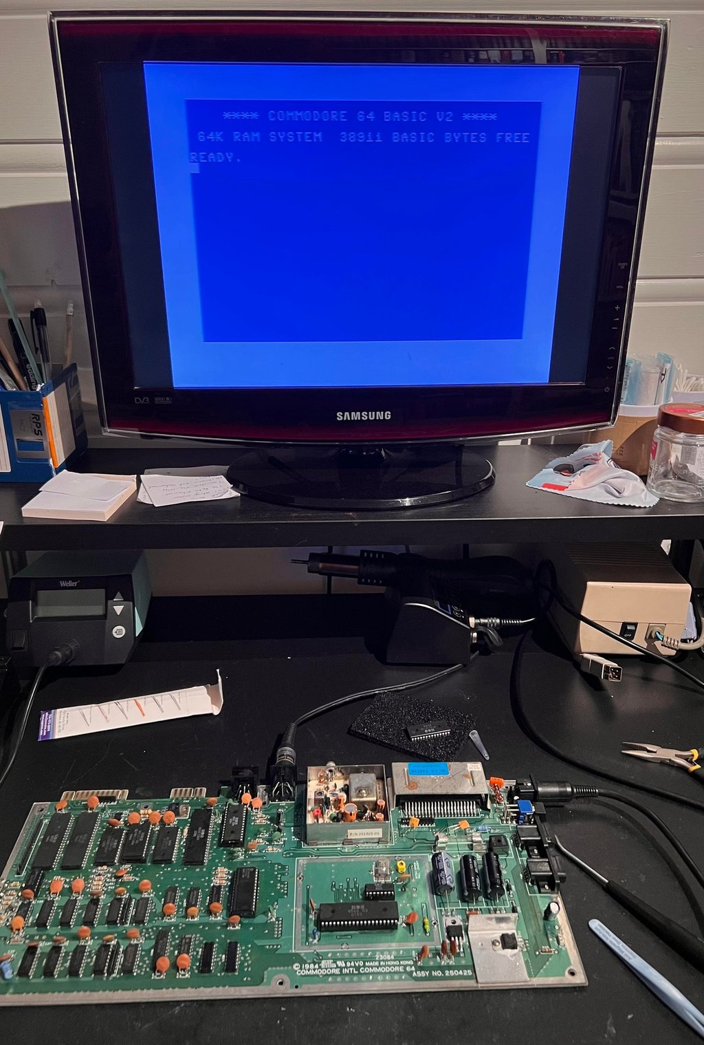
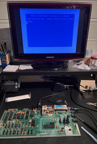
The switch is soldered back in to the mainboard. The result is... voltages are back! Yes! Now the voltages are set to +5 VDC and +12 VDC immediately.
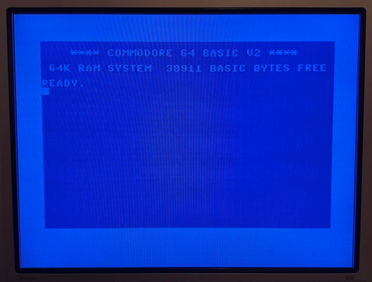
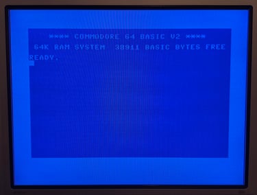
And now the well known blue screen appear! 38911 BASIC BYTES FREE!
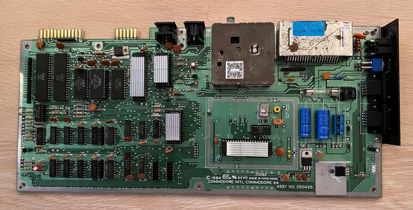
Replacing the electrolytic capacitors - Mainboard
There are not too many electrolytic capacitors on the mainboard, but they are old - almost 40 years old. So to replace these with new modern components is good refurbishing practice. The capacitor values can be found for mainboard assy 250425. Note: it is a good idea to remove the SID chip while doing this operation to prevent damaging it.
Below are pictures of the front nad back of the mainboard after new capacitors are installed.

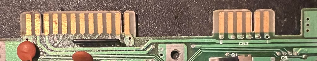
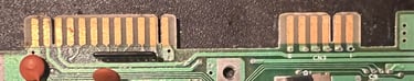
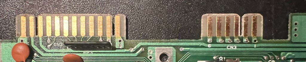
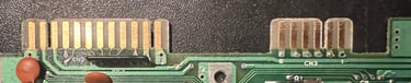
Cleaning the user- and datasette port
For the datasette to function, and for external peripherals connected to the user port, the connectors needs to be clean. After 40 years these are both dirty and oxidized. To remove this a normal rubber eraser (yes, finally you can use your smelly rubbers from the 80s) is used to remove most of the grease. Do not use abrasive tools such as a glass fibre pen since this will damage the copper. Finally the connectors are cleaned with isopropanol. Below are a pictures from before (top image) and after (bottom image) the cleaning of the connectors.
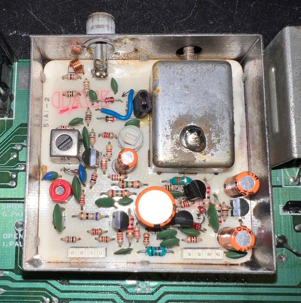
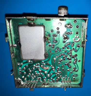
Replacing the electrolytic capacitors - RF modulator
As for the mainboard the electrolytic capacitors in the RF-modulator are almost 40 years old and should be replaced. There are only four electrolytic capacitors in this RF-modulator (Commodore P/N 251025-05), but the main challenge is to desolder the module from the mainboard without damaging either the RF-modulator or the mainboard. It is not that it is very complicated, but you need to be very careful. In the article “HOWTO – Desolder the RF-modulator” you can read and see how I do this.
Below is a picture of the RF-modulator before the desoldering operation.

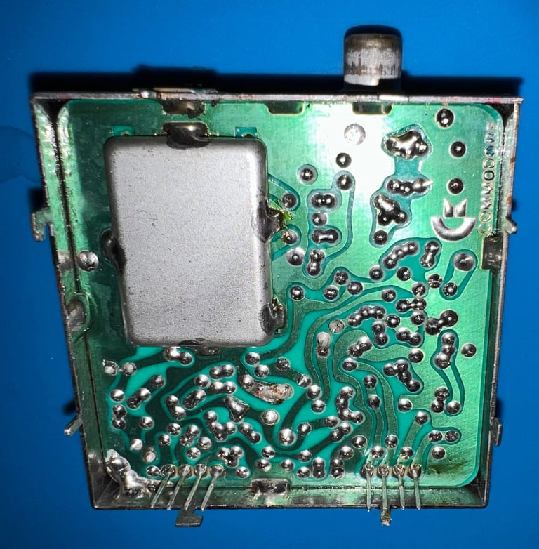
No pads or traces used for signals were damaged. But one of the pads used to solder the large pins to the mainboard loosened. This has no impact at all since there are three remaining large pins soldered to the mainboard – and also four tabs holding everything in place. As a matter of fact it is quite common that only three out of four pins are soldered to the mainboard.
Below is a picture of the mainboard after desoldering – no traces or pads damaged or lifted.

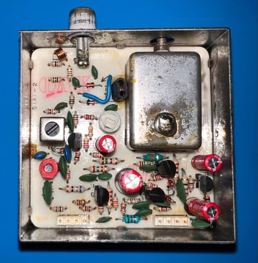
The four electrolytic capacitors are replaced according to the information in the capacitor reference bank. Below are some pictures of the RF-modulator with the new capacitors in place.

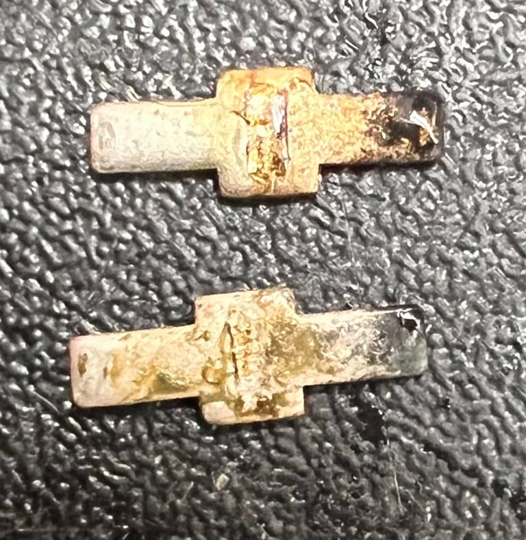
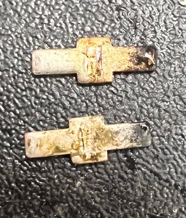
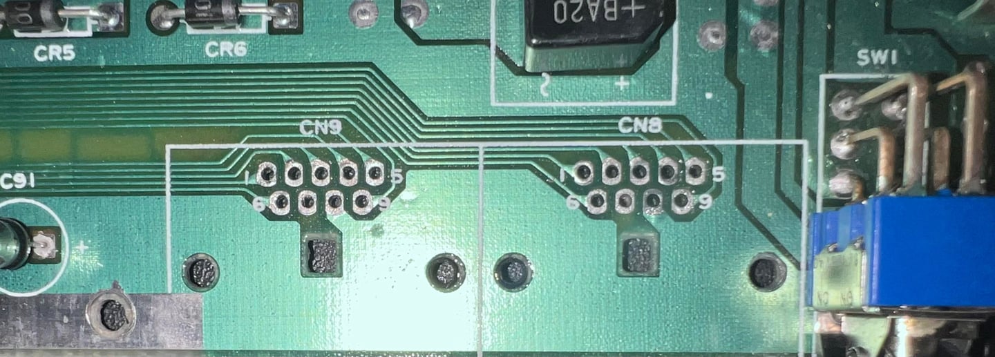
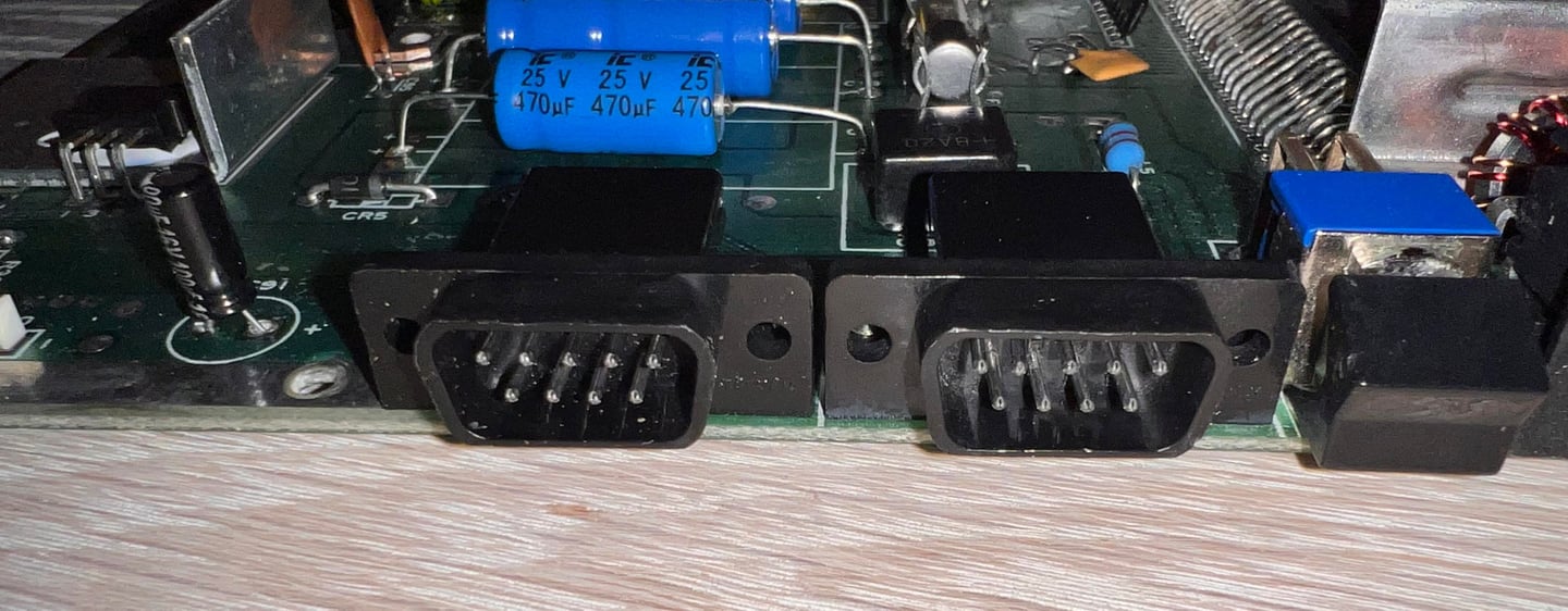
Replacing the joystick port connectors
Both connectors need replacement (CN8 and CN9). One of the ports is missing the “UP” direction pin, and on the other the surrounding plastic is broken preventing the joystick to be firmly in place.
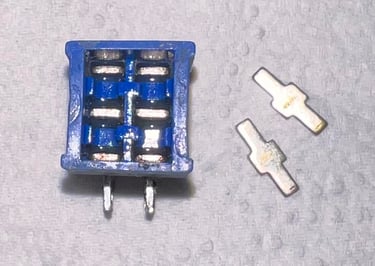
The two connectors are removed by first removing the four screws holding them in place. Then all the pins are carefully desoldered from the mainboard. No traces or pads were damaged during desoldering. See picture below.

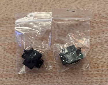
New joystick ports connectors are ordered from retroleum.co.uk which is a highly recommended webshop for Commodore 64 spare parts.

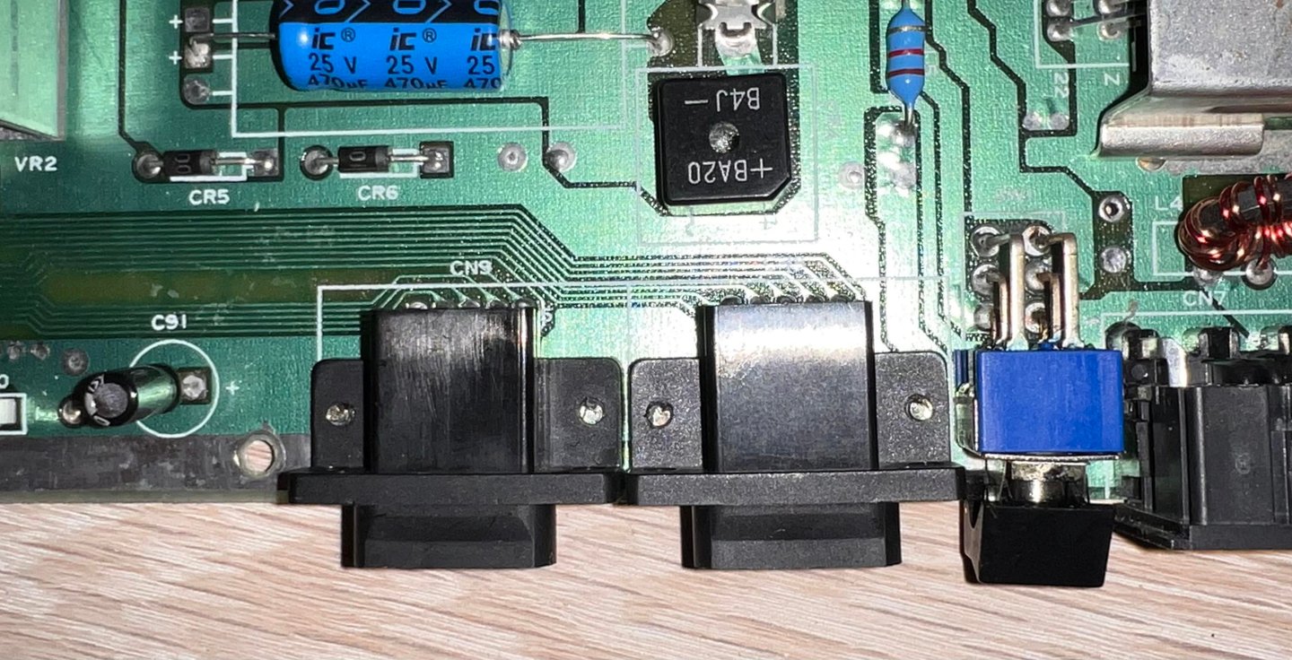
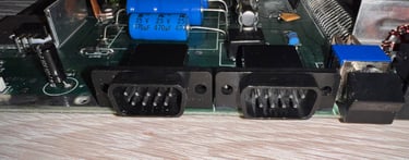
The two new port connectors are soldered back into CN8 and CN9.

Adding heatsinks on major custom chips
To increase the probability for a custom MOS chip to last longer heat sinks are added to some of the chips; the SID-, CPU-, PLA and VIC-II chip. Most of the heat is actually transferred from the IC pins to the mainboard, but the heat sinks on the top of the ICs will also dissipate heat to the surroundings.
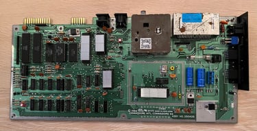
Below is a picture of the mainboard with heat sinks added.
Testing
Proof is in the pudding - does it work?
Testing is done through two main stages:
Testing the basic functionality and chips
Testing by using the machine playing demos, games etc. accessed by both floppy and datasette to verify correct operation
Basic functionality and chips
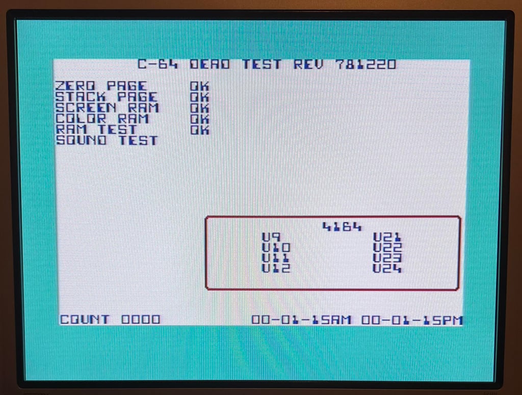
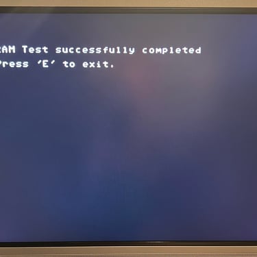
First test is done using the Dead Test Cartridge. This test doesn´t test all the functionality of the Commodore 64, but it does test the basic functionality of the major chips such as the CIA #1/2, CPU, VIC-II, PLA, RAM and SID. As the picture shows below the test is passed.
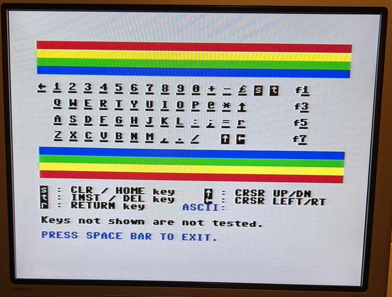
Next test is to power the Commodore 64 to the blue boot up screen and also check the keyboard to make sure all keys works as they should. The test is passed; all keys works and 38911 BASIC Bytes Free.

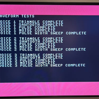
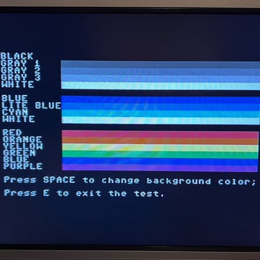
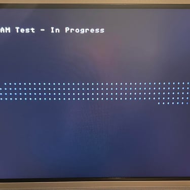
The basic functions of the VIC-II, SID and RAM is tested with 64 Doctor. Note that this is to be considered as basic functionality - more advanced (?) functionality such as sprite handling / collision detection / advanced audio will be tested later. But the basic tests pass without any detected faults (click to enlarge).
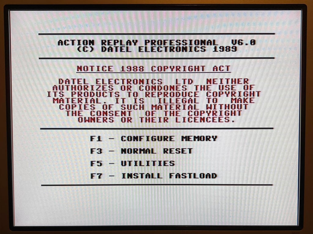
Last basic check before moving to more extensive testing is checking the cartridge. This is done by using the Action Replay VI. Result is that the test is passed.
Extended testing
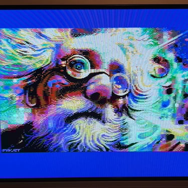
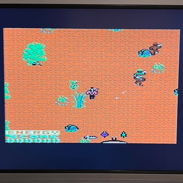
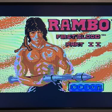
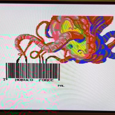
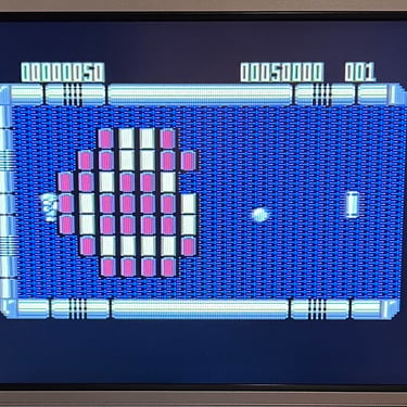
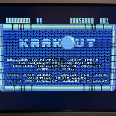
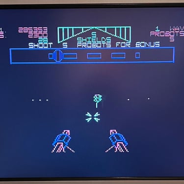
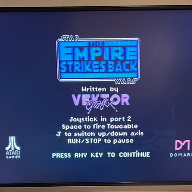
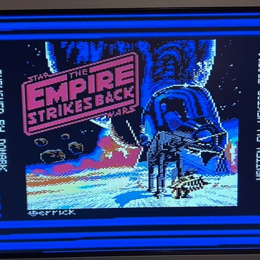
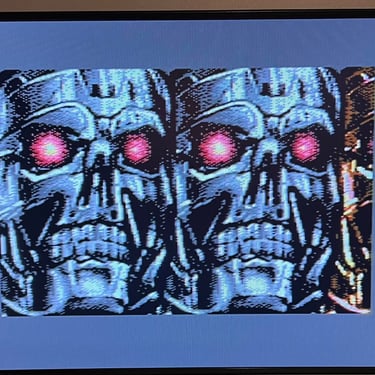
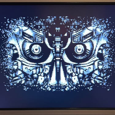
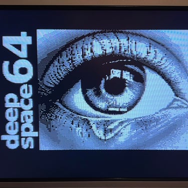
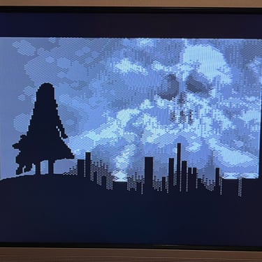
Knowing that the basic functionality of the machine works I continue the testing by using the Commodore 64 for normal operations; playing some games, watching demos, loading from datasette and floppy and using a cartridge. I can not find any issues with this machine. I also pay special attention to the video to make sure that there are no glitches in the graphics - I can´t see any abnormalities. Below is a gallery with pictures from the testing.

Final result
"A picture worth a thousand words"
Below is a collection of the final result from the refurbishment of this C64. Hope you like it! Click to enlarge!


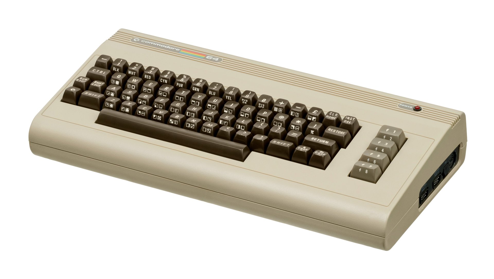
Banner picture credits: Evan-Amos