
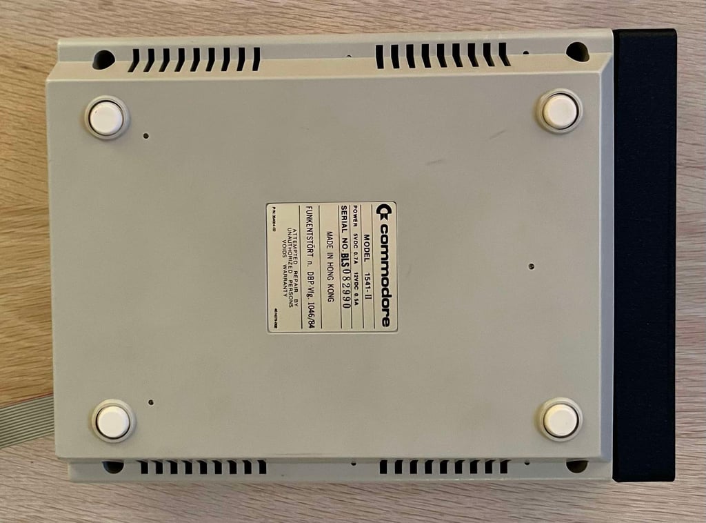
Commodore 1541-II
Ser. No. BLS082990
Assy 340503
Fab No. 355124 (REV 9)
Chinon
Starting point
This 1541-II floppy drive is in here not just for the ordinary refurbish, but also for a major upgrade: equipping the floppy drive with the MeGALoDOS speeder. This will enable the drive to read floppies at incredible speed.
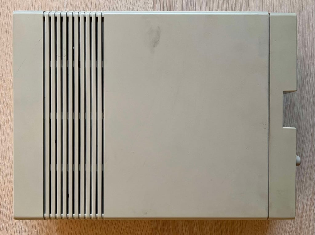
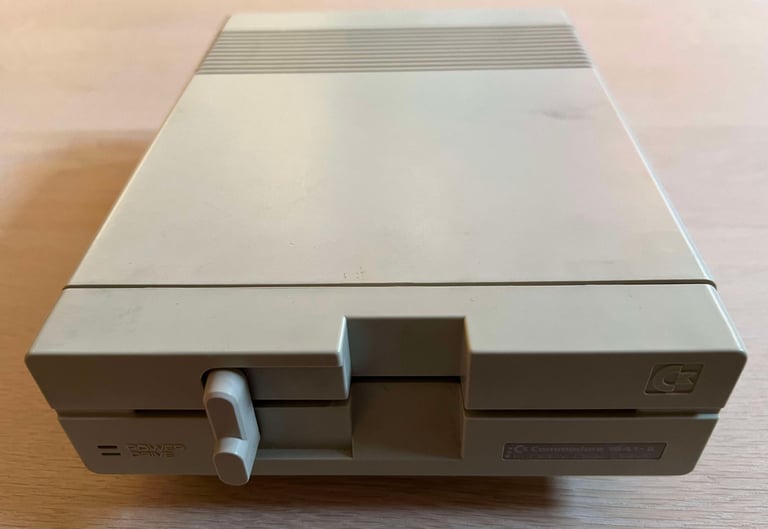
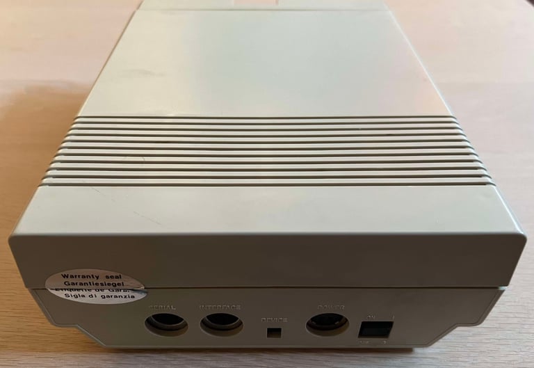
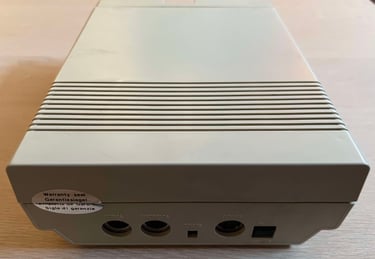
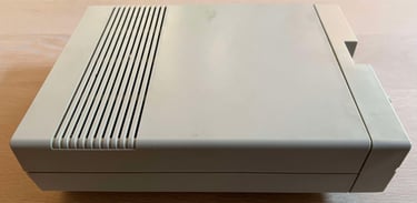
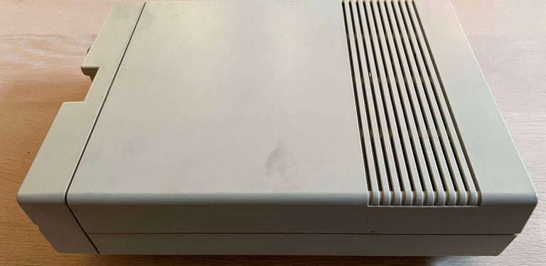
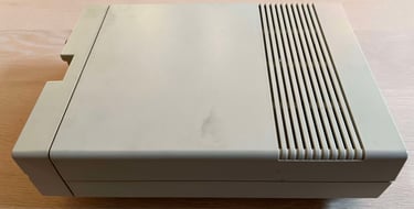
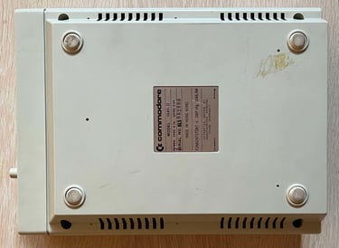
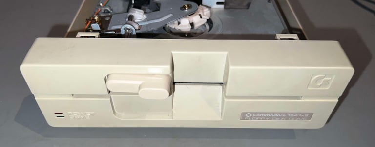
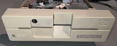
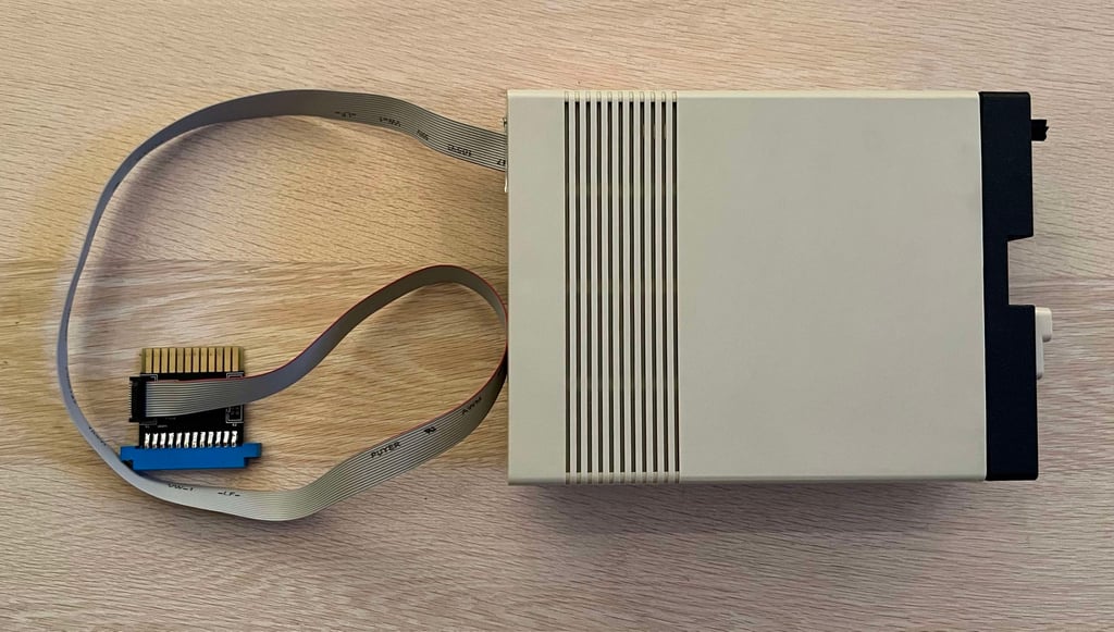
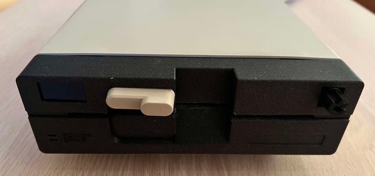
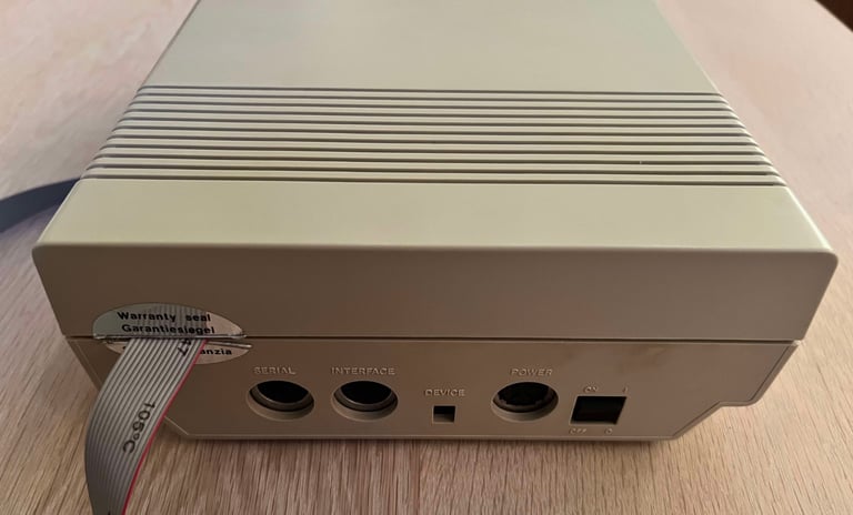
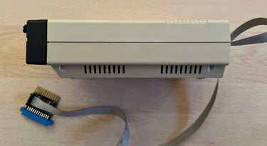
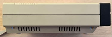
From the outside the floppy drive looks to be in fine condition. There are some dust and grease on the covers, but it is marginal. The ports seems to be fine, the open/close lever at the front works fine and the power switch at the back appear to be in mechanical good condition. It is slightly yellowed, but not severely. The warranty seal at the back is broken.
Below are some pictures of the 1541-II floppy drive before the refurbishment.


Refurbishment plan
The refurbishment plan for this 1541-II (order can vary and some of the tasks will be done in parallell):
STAGE #1: Cleaning, inspection and initial testing
- Initial testing #1
- Clean the interior and lubricate moving parts
- Initial testing #2
- Clean and inspect the PCBs (mainboard)
- Refurbish the casing (cleaning)
STAGE #2: Installation of MeGALoDOS
- Prepare the installation of the MeGALoDOS v1.42F mainboard
- Prepare the installation of the VIA adapter
- Install MeGALoDOS and VIA adapter on the mainboard
- Install the display, rotary encoder and POWER/LED on a 3D printed front
STAGE #3: Testing
- Verify drive operation by testing the drive with the C64G equipped with SuperKernal.
The plan can be updated during the refurbishment process. Sometimes I discover areas that needs special attention.
STAGE #1:
Cleaning, inspection and initial testing
Initial test #1
A quick initial test is performed. The 1541 floppy ROM contains a small initialising program which is executed on power-on. This is the only test done before the refurbish. The rest of the initial testing will be done at later of stage #1. As can be seen in the table below the initial test #1 passed OK.
Disassembly (1/2)
Before the refurbishment can start the floppy drive needs to be disassembled. Disassembling the 1541-II is straightforward. First, the four screws at the bottom are removed (Phillips 3 x 10 mm). But, it turns out the one of the screws are missing. Not a big deal, but this will be replaced later.
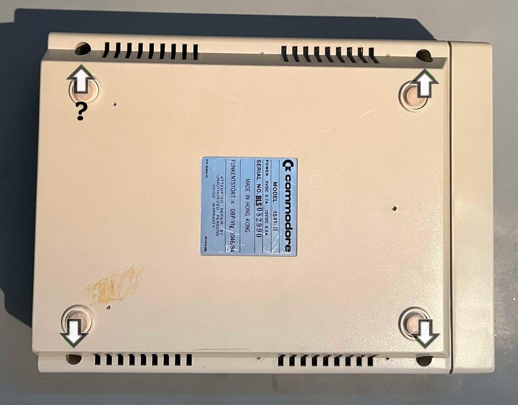

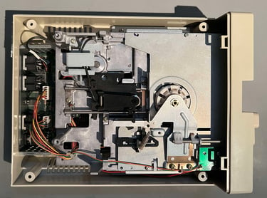
With the screws out of the way the top cover is lifted from the bottom cover. As can be seen from the picture below, the inside looks good. At first glance this drive seems to be in fine condition from a mechanical point of view. There are of course some dust and grease, but nothing more than is to be expected.
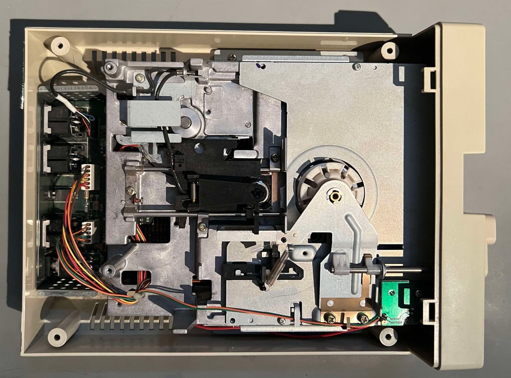
To detach the front the open/close lever is removed by pulling it firmly towards you. Keep in mind that this is old and brittle plastic so avoid brute force.
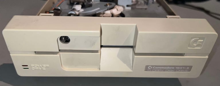
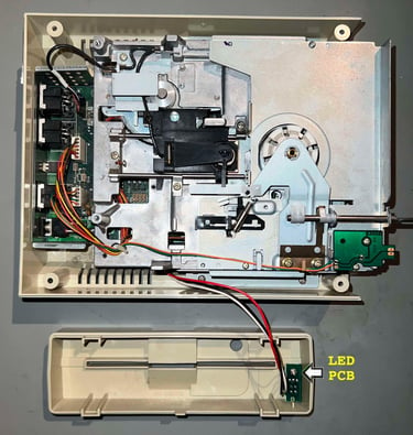
When lifting the front cover away mind the cable attached to the small LED PCB. It is good practice to remove the small screw holding the LED PCB, detach the PCB and put the screw back in without the PCB (prevents you from loosing the screw).

Cleaning the R/W head and lubricating the rails
The floppy drive mechanism is a Chinon FZ-501M (Rev A) - serial number 10431711.
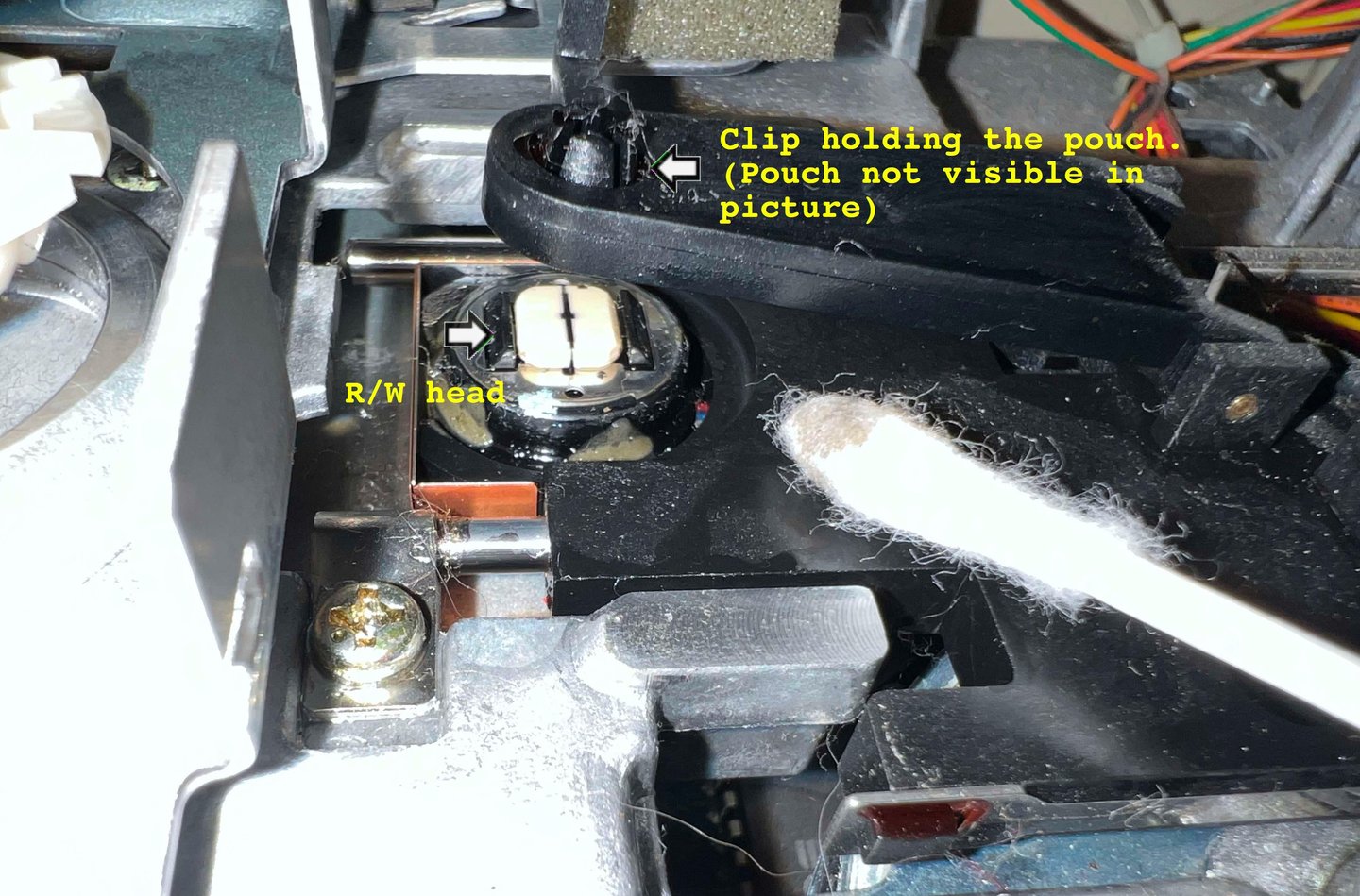
With the floppy drive partly disassembled the R/W head can be cleaned. With some isopropanol and a Q-tip the R/W head is cleaned. WARNING: Be careful when cleaning and be patient. The R/W head is likely to be covered with a thin residue of "stuff" from old floppies. This "stuff" will come off with isopropanol, but clean it off gently. Also, keep in mind that above the R/W head is a small pouch which can easily be damaged if not careful. This couch push the magnetic floppy down on the R/W head so you do not want to damage this.

For the R/W head to cover all the tracks 1-35 of the floppy the rails must be without impediments. Therefore the rails are cleaned with isopropanol (and a Q-tip) and then lubricated with some machine oil. To get access to the rails the R/W head can be gently pushed for the far right and far left.

Initial test #2
Now that the R/W head is cleaned, and the rails are lubricated, the second part of the initial testing can commence. To perform the second part of the test the 1541 Test & Diagnostic cartridge from World of Jani is used. The 1541-II floppy drive is connected to a C64 running this cartridge and several tests are performed.
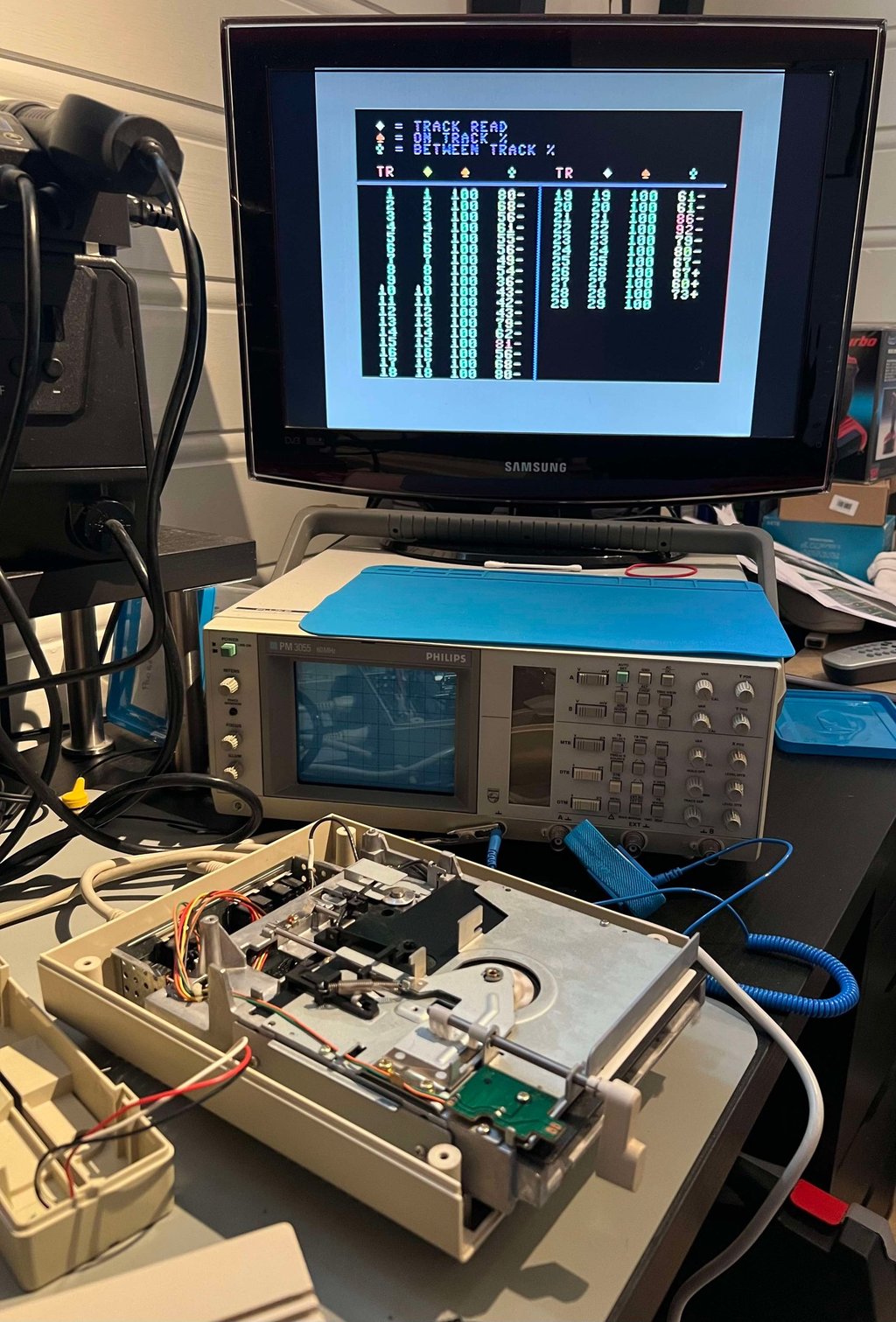
All the tests pass without any issues. See table and picture gallery below (click to enlarge).
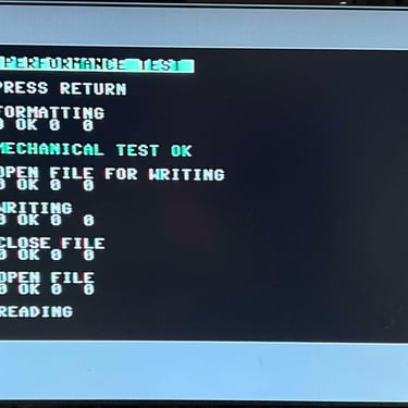
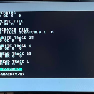
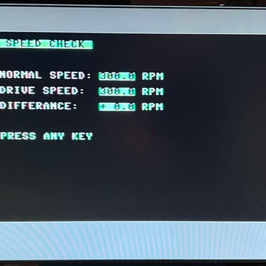
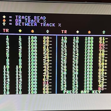
Disassembly (2/2)
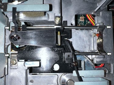
Now that the initial testing is complete the rest of the floppy drive is disassembled. Next step is to unmount the whole disk mechanism. This is fastened with four 3 x 7 mm screws - two on each side of the drive mechanism. See arrows in picture below.
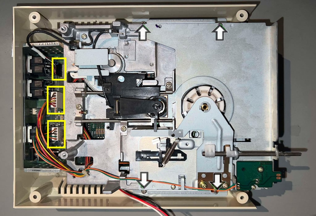
Before lifting the drive mechanism out of the bottom cover the three cable connectors at the PCB are removed. Note the direction of these - if they are inserted "upside down" on reinstallation you are in trouble...
When the drive mechanism is removed the PCB is exposed in all its glory. And it looks to be in good condition. There is quite some dust and grease, but I can not see anything intimidating.
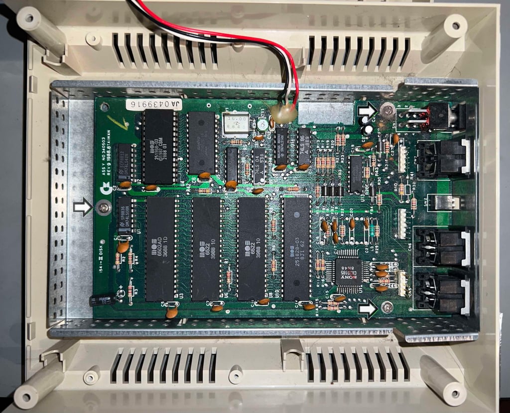
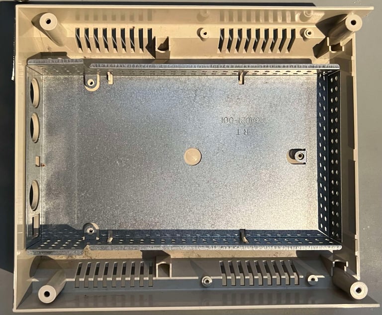
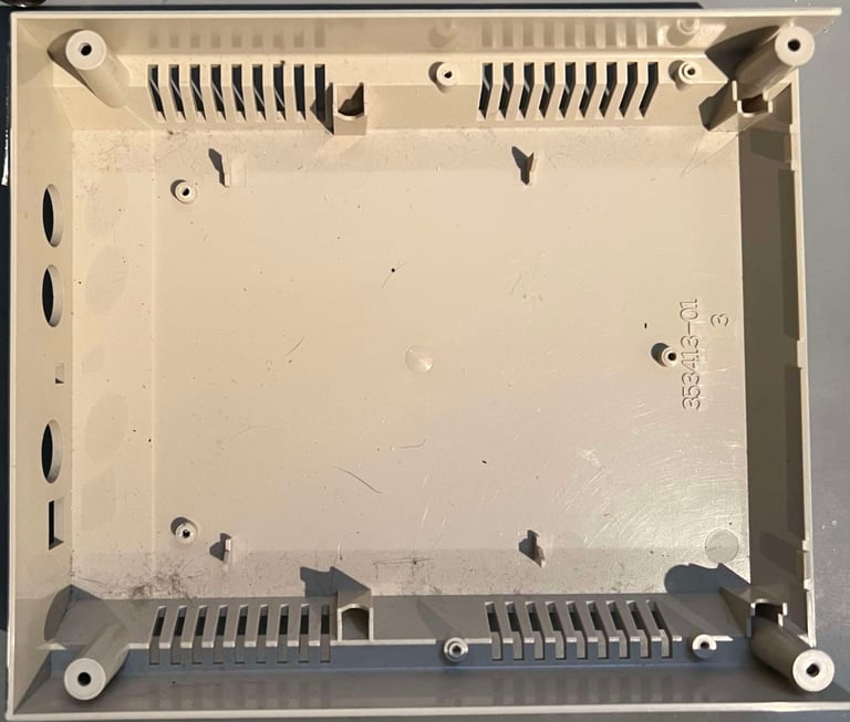
The three screws ( 3 x 9 mm) holding the PCB to the bottom cover are removed. Then PCB is lifted off, the bottom cover is now free and the disassembly is complete.

Cleaning and inspection the PCB(s)
The floppy drive consists of two main PCBs:
Mainboard controlling the drive and communication to the Commodore 64. Mounted in the bottom cover.
Additional board controlling the motor- and drive mechanics. Mounted on the underside of the drive mechanism.
The mainboard controlling the drive and communication to the C64 seem to be in good condition, but it is dirty. I can not see any sign of damage, such as corrosion or leaking capacitors. Neither can I see any sign of rework. See pictures below.
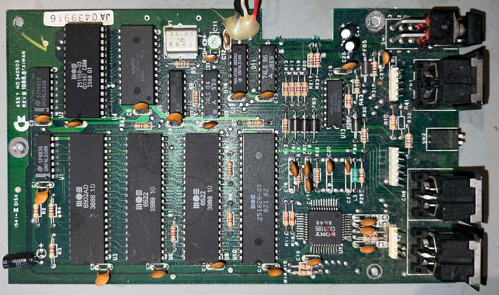
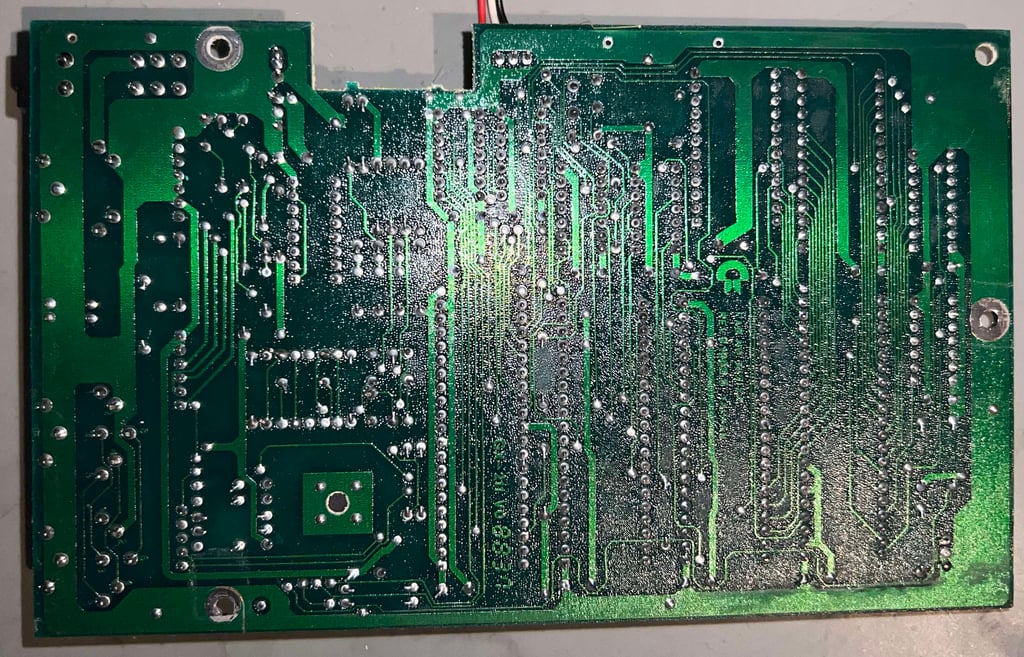
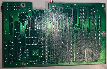
The PCB is cleaned properly with isopropanol and an ESD safe brush. This PCB is marked with "Assy 340503/Fab No. 355124/GX-211 VO 8837". From the table below showing the ICs found on the mainboard I think its fair to say that this 1541-II floppy drive was assembled sometime in the autumn of 1988.
STAGE #2:
Installation of MeGALoDOS
Removing the DOS ROM socket (U4)
The DOS ROM in the 1541-II is installed in a socket. Normally, this is a good thing, but the MeGALoDOS PCBA requires the socket to be removed and the DOS ROM IC to be directly soldered to the mainboard. The reason for this is that the space between the top of the 1541-II mainboard and the bottom the of Chinon drive mechanics is very limited.
Desoldering the socket at is done without any damage to traces or pads. See picture below.
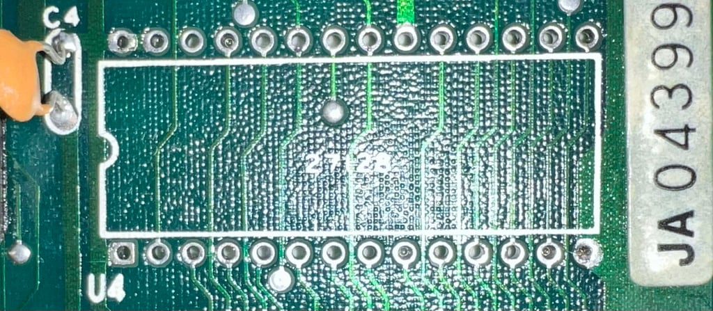

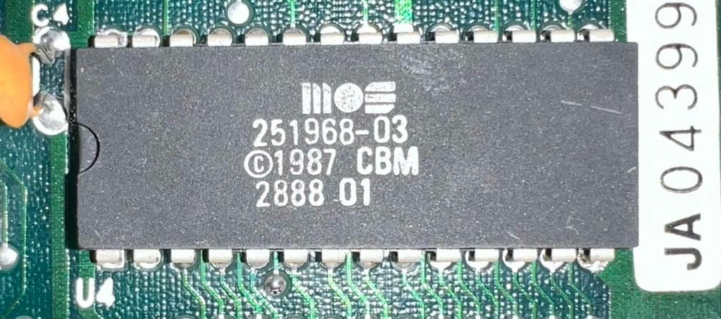
The MOS 251968-03 DOS ROM is soldered back in, this time without a socket. The soldering operation is done without any issues. NOTE: with the DOS ROM soldered back in the mainboard is powered on. The drive is not re-assembled but the LED does show that the initial test is working fine. The DRIVE light is on for a while and then is shut off. Below is a picture of the DOS ROM soldered directly to the mainboard.
Adding a socket to the MOS 6502 CPU (U3)
In contrast to the DOS ROM which has to be soldered directly onto the mainboard, the 6502 CPU has to be socketed. This will allow the MeGALoDOS PCB to hover over the DOS ROM. The 6502 CPU is desoldered without any damage to traces or pads. See picture below.
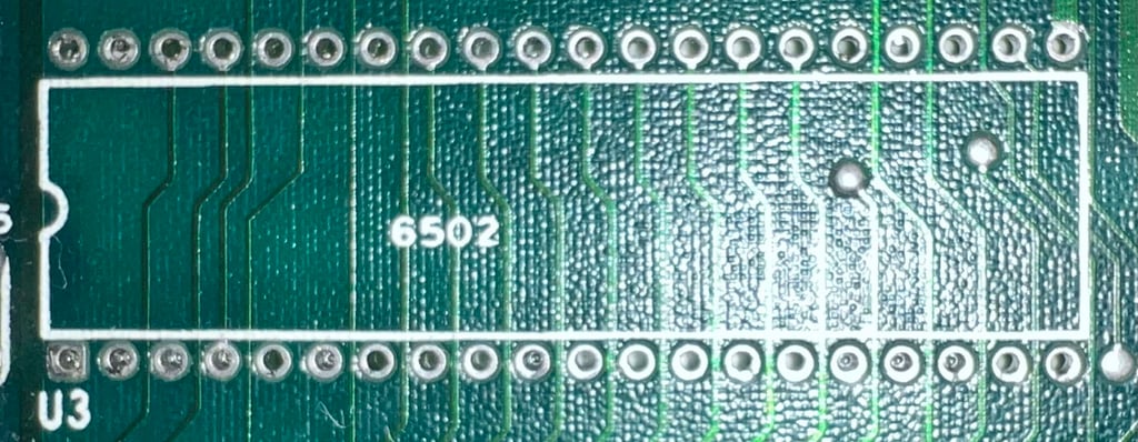
A machine pin IC socket is soldered in position U3. NOTE: the 6502 CPU is installed back in the socket and mainboard is powered on. The drive is not re-assembled but the LED does show that the initial test is working fine. The DRIVE light is on for a while and then is shut off.
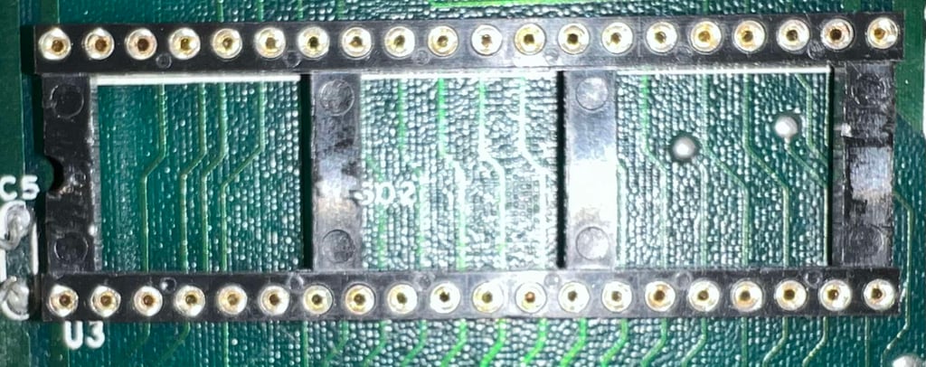
Desoldering the MOS 6522 VIA #1 (U6)
The VIA #1 IC located at U6 need to be desoldered so that the VIA adapter can be soldered instead. The IC is desoldered without any damage to traces or tracks. See picture below.
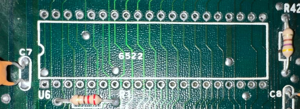
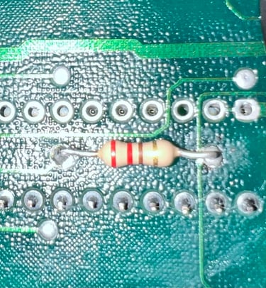
But for the VIA adapter to fit, both the capacitor (C7) and resistor (R1) must be desoldered and soldered on the backside of the PCB. See pictures below.
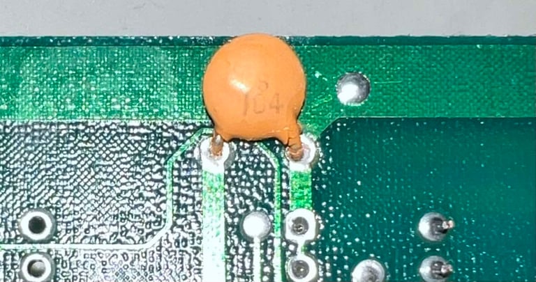

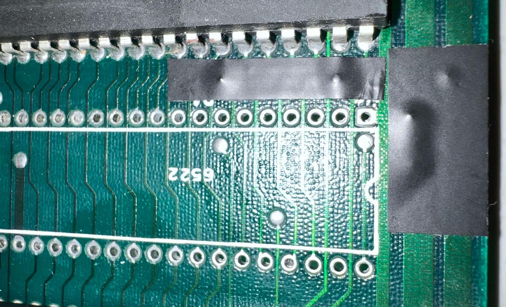
To make sure that the solder points on the top side does not short circuit they are insulated with some tape.

Soldering the VIA adapter
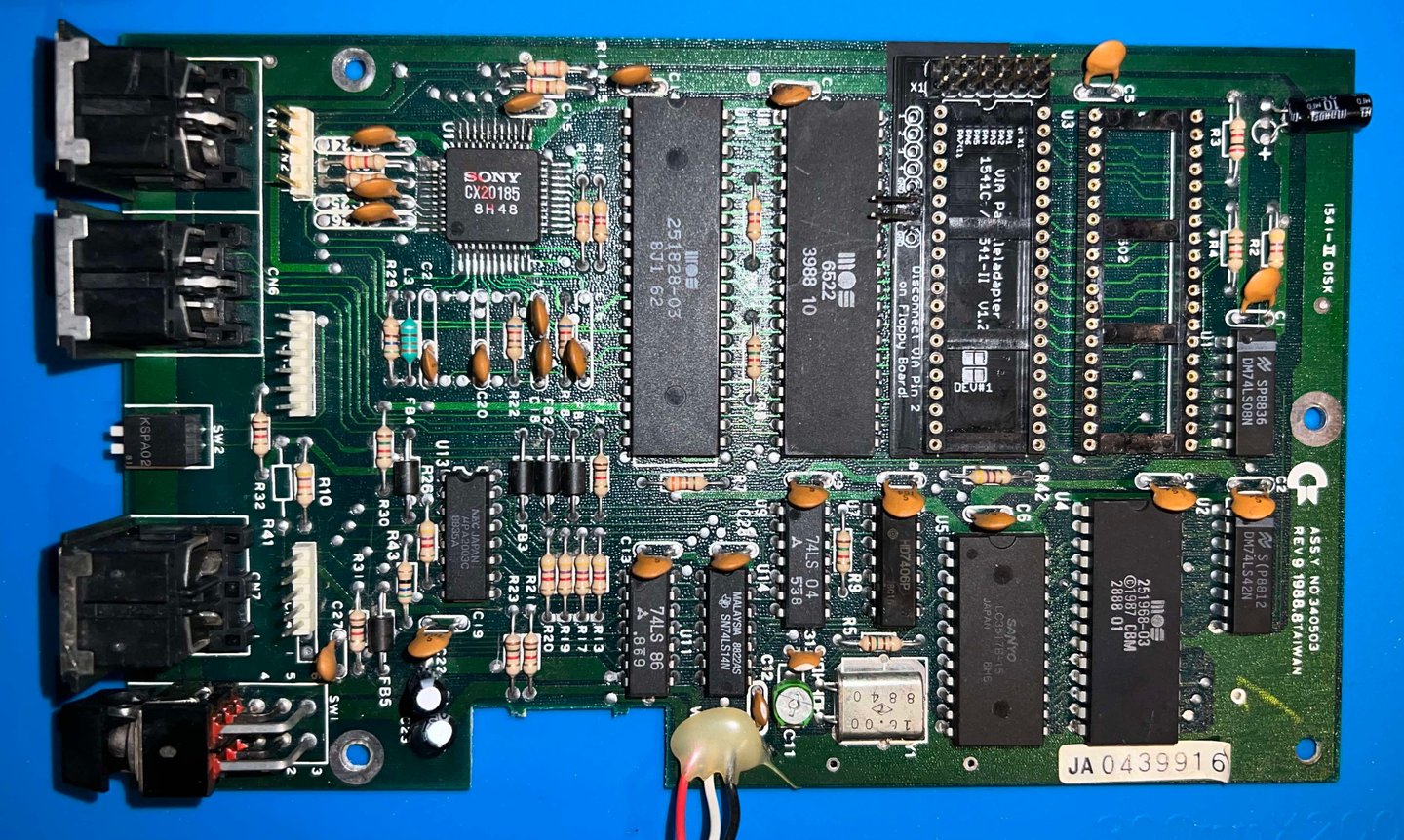
The VIA adapter is soldered to the mainboard. With the capacitor and resistor out of the way the adapter is flush with the PCB. Below is a picture of the 1541-II mainboard with the VIA adapter installed.
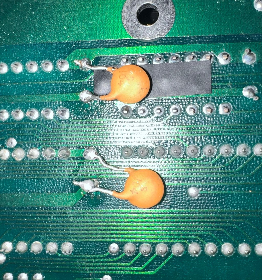
Moving C2 and C4 to the backside
I recognise that for the MeGALoDOS to fit perfectly the C2 and C4 is moved to the backside of the PCB. It doesn´t look so nice, but it does the job!

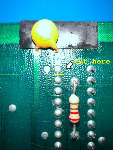
Cutting the trace between PIN #1 and #2 on VIA#1 (U6)
The MeGALoDOS require the trace between pin #1 and pin #2 on the VIA#1 (U6). With a sharp scalpel the trace is cut, and with the a multimeter the cut is verified as there are no longer a connection between the two pins. See picture below.

Installing the ICs and MeGALoDOS PCB
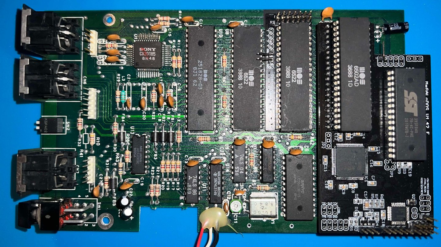
Now everything is ready for the ICs and the MeGALoDOS to be installed on the mainboard. Below is a picture of the mainboard with these in place.
Installing the display, rotary encoder and POWER/DRIVE LED
First of all a new 3D printed front is made. The front will replace both the 1541-II bezel, the door handle and add a knob for the rotary encoder. You can find the 3D files for the MeGALoDOS speeder at printables.com.
Below are some pictures of the 3D printed parts; the front bezel, the rotary encoder knobs and the door handle.

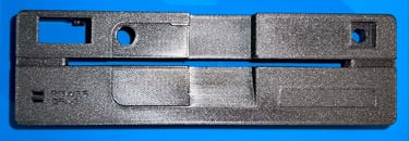
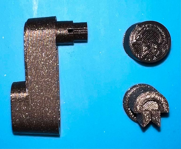
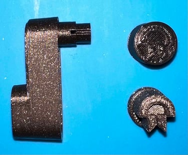
The display is modified sightly to make it fit in the 3D printed bezel. With some hot air (from a hair dryer) and some prying tools, the display is detached from the PCB.
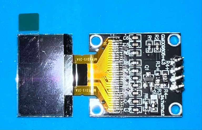
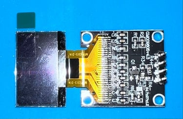
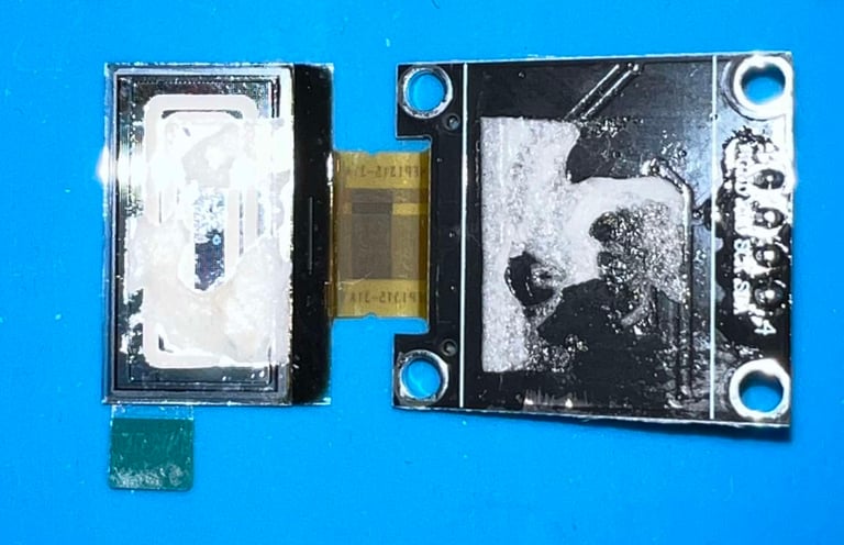

Installing the display, rotary encoder and LED into the 3D printed bezel is not trivial. I do not have pictures of the process unfortunately, but here is a short written summary of what I had to do:
The pin header on the display was desoldered and removed. Instead, four thin cables were soldered to the display PCB
The display screen (backside) is glued to the bezel
The original drive LED is removed from the small PCB. This is to make room for the new dual colour LED attached to the MeGALoDOS mainboard
Between the bottom cover and the internal drive support frame 1 mm spacers are added. This is to make sure that the flywheel does not touch the top of the ICs on the MeGALoDOS mainboard
The two cables used for device selection (8, 9, 10 and 11) are soldered directly to the MeGALoDOS pins. On the VIA expander the Dupont connectors are still used.
The 3D printed door handle I could not get to fit unfortunately without risking damage to the internal drive mechanism.
STAGE #3:
Testing and verification
The purpose of this stage is to test, and verify, that the 1541-II floppy disk drive works as it should. Basic functionality were tested in stage #1 and now everything is re-tested and verified. A combination of software tools are used in this process - please see description of tools.
In the table below are the results from the testing using normal CBM DOS and CBM Kernal.
In the table below are the results from testing using selected speeder ROMs on both CPU and drive side. Software being used is the 64´er floppy-speed-tester.
Final result
"A picture worth a thousand words"
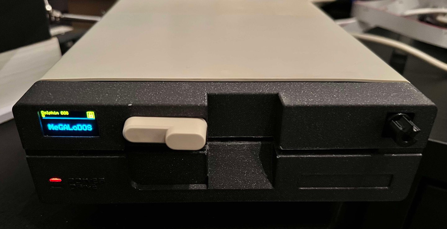
Below is a collection of the final result from the refurbishment of this 1541-II floppy drive. Hope you like it! Click to enlarge!




Banner picture credits: DoorwayToDorkness
